5
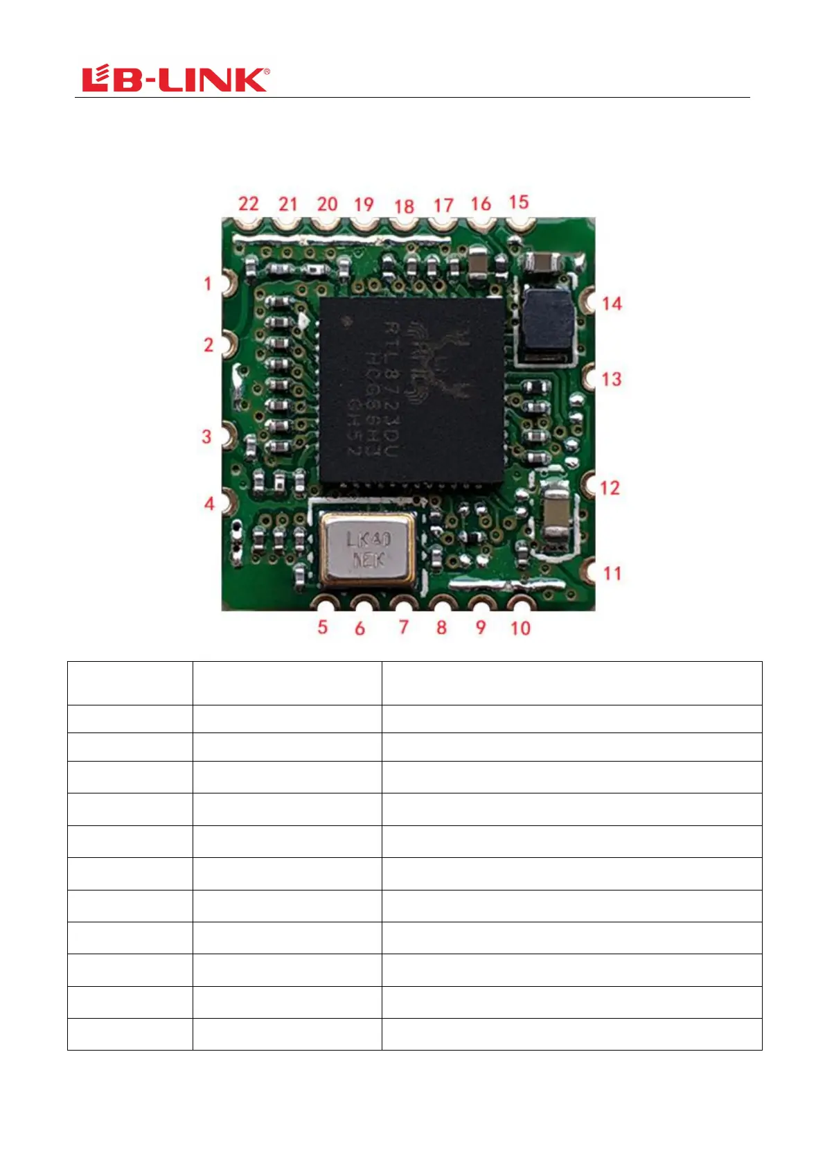
4. Pin Assignments
Figure 4
Pin Assignments
(Top view)
Pin No. Pin Name Description
1 GND Grond
2 RF-S0 WLAN/BT RF TX/RX signal port 0
3 RF-S1
4 GND Grond
5 BT_PCM_IN General Purpose Input/Output Pin
6 BT_PCM_OUT General Purpose Input/Output Pin
7 BT_PCM_SYNC General Purpose Input/Output Pin
8 BT_PCM_CLK General Purpose Input/Output Pin
9 BT_WAKE_HST Chip wakeup host
10 HST_WAKE_BT host wakeup Chip
11 VDD33 The power input 3.3V
WLAN/BT RF TX/RX signal port 1(No signal transmission)