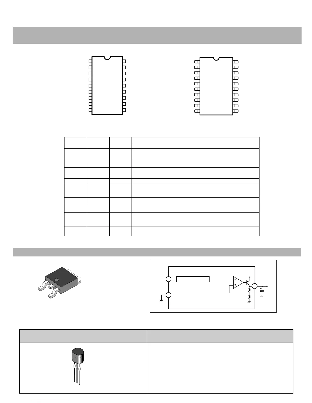
PIN FUNCTIONS
PIN DIP-18 PIN SO-20 NAME DESCRIPTION
11 12 COMP E/A output to be used for frequency compensation
10 11 INH A logic signal (active high) disables the device (sleep mode operation).
If not used it must be connected to GND; if floating the device is disabled.
9 10 BOOT A capacitor connected between this pin and the output allows to drive the
internal D-MOS.
18 20 SYNC Input/Output synchronization.
7,8 8,9 Vcc Not regulated DC input voltage
2,3 2,3 OUT Stepdown regulator output.
12 13 VFB Stepdown feedback input. Connecting directly this pin to the output 3.3V
and 5.1V are obtained; a voltage divider is requested for higher output
voltages. For voltage below 3.3V see note **
16 18 V5.1 Reference voltage externally available.
4,5,6
13,14,15
4,5,6,7
14,15,16,17
GND Signal ground
1 1 OSC An external resistor connected between the unregulated input voltage and
Pin 1 and a capacitor connected from Pin 1 to ground fixes the switching
frequency. (Line feed forward is automatically obtained)
17 19 SS Soft start time constant. A capacitor connected between this terminal and
ground determinates the soft start time.
1. Vcc
2. GND
3. OUTPUT
 Loading...