5 6
QF01
: µ: µ
: µ: µ
: µPD78076 MAIN
SYMBOL PIN PADCELL DESCRIPTION
RC
fil
1 E029 PLL loop filter input
V
ref
2 E029 decoupling internal reference voltage output
V
DDA
3 E008 analog supply voltage
V
SSA
4 E004 analog ground
IECIN1 5 E007 high sensitivity IEC input
IECIN0 6 IPP04 TTL level IEC input
IECSEL 7 IUP04 select IEC input 0 or 1 (0 = IECIN0; 1 = IECIN1); this input has an internal pull-up
resistor
IECO 8 OPFH3 digital audio output for optical and transformer link
IECOEN 9 IUP04 digital audio output enable (0 = enabled; 1 = disabled/3-state); this input has an
internal pull-up resistor
TESTB 10 IPP04 enable factory test input (0 = normal application; 1 = scan mode)
TESTC 11 IPP04 enable factory test input (0 = normal application; 1 = observation outputs)
UNLOCK 12 OPP41A PLL out-of-lock (0 = not locked; 1 = locked); this output can drive an LED
FS32 13 OPP41A indicates sample frequency = 32 kHz (active LOW); this output can drive an LED
FS44 14 OPP41A indicates sample frequency = 44.1 kHz (active LOW); this output can drive an LED
FS48 15 OPP41A indicates sample frequency = 48 kHz (active LOW); this output can drive an LED
CHMODE 16 OPP41A use of channel status block (0 = professional use; 1 = consumer use); this output
can drive an LED
V
DDD2
17 E008 digital supply voltage 2
V
SSD2
18 E009 digital ground 2
RESET 19 IDP09 initialization after power-on, requires only an external capacitor connected to V
DDD
;
this is a Schmitt-trigger input with an internal pull-down resistor
PD 20 IPP04 enable power-down input in the standby mode (0 = normal application; 1 = standby
mode)
CTRLMODE 21 IUP04 select microcontroller/stand-alone mode (0 = microcontroller; 1 = stand-alone); this
input has an internal pull-up resistor
LADDR 22 IPP04 microcontroller interface address switch input (0 = 000001; 1 = 000010)
LMODE 23 IPP09 microcontroller interface mode line input
LCLK 24 IPP09 microcontroller interface clock line input
LDATA 25 IOF24 microcontroller interface data line input/output
STROBE 26 IDP04 strobe for control register (active HIGH); this input has an internal pull-down resistor
UDAVAIL 27 OPF23 synchronization for output user data (0 = data available; 1 = no data)
TESTA 28 IPP04 enable factory (scan) test input (0 = normal application; 1 = test clock enable)
COPY 29 OPP41A copyright status bit (0 = copyright asserted; 1 = no copyright asserted); this output
can drive an LED
INVALID 30 IOD24 validity of audio sample input/output (0 = valid sample; 1 = invalid sample); this pin
has an internal pull-down resistor
DEEM 31 OPF23 pre-emphasis output bit (0 = no pre-emphasis; 1 = pre-emphasis)
MUTE 32 IUP04 audio mute input (0 = permanent mute; 1 = mute on receive error); this pin has an
internal pull-up resistor
I
2
SSEL 33 IUP04 select auxiliary input or normal input in transmit mode
SDAUX 34 IPP04 auxiliary serial data input; I
2
S-bus
SD 35 IOF24 serial audio data input/output; I
2
S-bus
WS 36 IOF24 word select input/output; I
2
S-bus
SCK 37 IOF29 serial audio clock input/output; I
2
S-bus
I
2
SOEN 38 IUP04 serial audio output enable (0 = enabled; 1 = disabled/3-state); this input has an
internal pull-up resistor
SYSCLKI 39 IPP09 system clock input (transmit mode)
SYSCLKO 40 OPFA3 system clock output (receive mode)
V
SSD1
41 E009 digital ground 1
V
DDD1
42 E008 digital supply voltage 1
CLKSEL 43 IUP04 select system clock (0 = 384f
s
; 1 = 256f
s
); this input has an internal pull-up resistor
RC
int
44 E029 integrating capacitor output
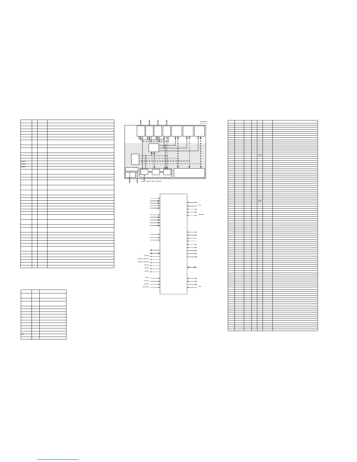
Q507/Q509 : DSP56004
QD03/QD53 : TDA1541A/S2
Q304 : TDA1315H
Pin No. Port Name Function In/Out Active To/From Description
1 STRB P120 Out Hi
---
---
PINNING
Note
1. See Table 1 data selection input.
SYMBOL PIN DESCRIPTION
LE/WS
(1)
1
latch enable input/ word select
input
BCK
(1)
2 bit clock input
DATA L
/D ATA
(1)
3
data left channel input/ data
input (selected format)
DATA R
(1)
4 data right channel input
GND(A) 5 analog ground
AOR 6 right channel output
DECOU 7 to 13 decoupling
GND (D) 14 digital ground
V
DD2
15 −15 V supply voltage
COSC 16,17 oscillator
DECOU 18 to 24 decoupling
AOL 25 left channel output
V
DD1
26 −5 V supply voltage
OB/TWC
(1)
27 mode select input
V
DD
28 +5 V supply voltage
Y Data
Memory*
X Data
Memory*
Program
Memory*
Program Control Unit
24-Bit
DSP56000
Core
OnCE
TM
Port
PLL
Clock
Gen.
4 9 5 29
16-Bit Bus
24-Bit Bus
Interrupt
Control
4
IRQA
,
IRQB, NMI
,
RESET
43
Address
Generation
Unit
PAB
XAB
YAB
GDB
PDB
XDB
YDB
General
Purpose
Input/
Output
External
Memory
Interface
(EMI)
Serial
Audio
Interface
(SAI)
Serial
Host
Interface
(SHI)
*Refer to Table 1 for memory configurations.
Internal
Data
Bus
Switch
Program
Decode
Controller
Program
Address
Generator
Data ALU
24 × 24 + 56 → 56-bit MAC
Two 56-Bit Accumulators
MA0ÐMA14
MD0ÐMD7
MWR
MA17/MCS1/MRAS
MA16/MCS2/MCAS
GND
Q
V
CCQ
RESET
MODA/IRQA
MODB/IRQB
MODC/NMI
SS/HA2
MISO/SDA
SCK/SCL
GND
S
V
CCS
WSR
SCKR
SDI0
DSCK/OS1
DSI/OS0
DSO
DR
OnCEª
Port C
Port B
Port A
External Memory
Mode/Interrupt
80 signals
Serial Host
Rec0
SDO1
Tran1
WST
SCKT
SDO0
Tran0
Interface
MRD
MCS0
Serial Audio
Interface
Interface
MOSI/HA0
SDO2
Tran2
SDI1
Rec1
GPIO0ÐGPIO3
GPIO
HREQ
V
CCP
GND
P
PCAP
PLL
PINIT
MA15/MCS3
EXTAL
GND
A
V
CCA
GND
D
V
CCD
Reset
Port
Power Inputs
Ground
Control
2
2
3
3
4
2
3
8
4
15
DSP56004
 Loading...