1-221-21
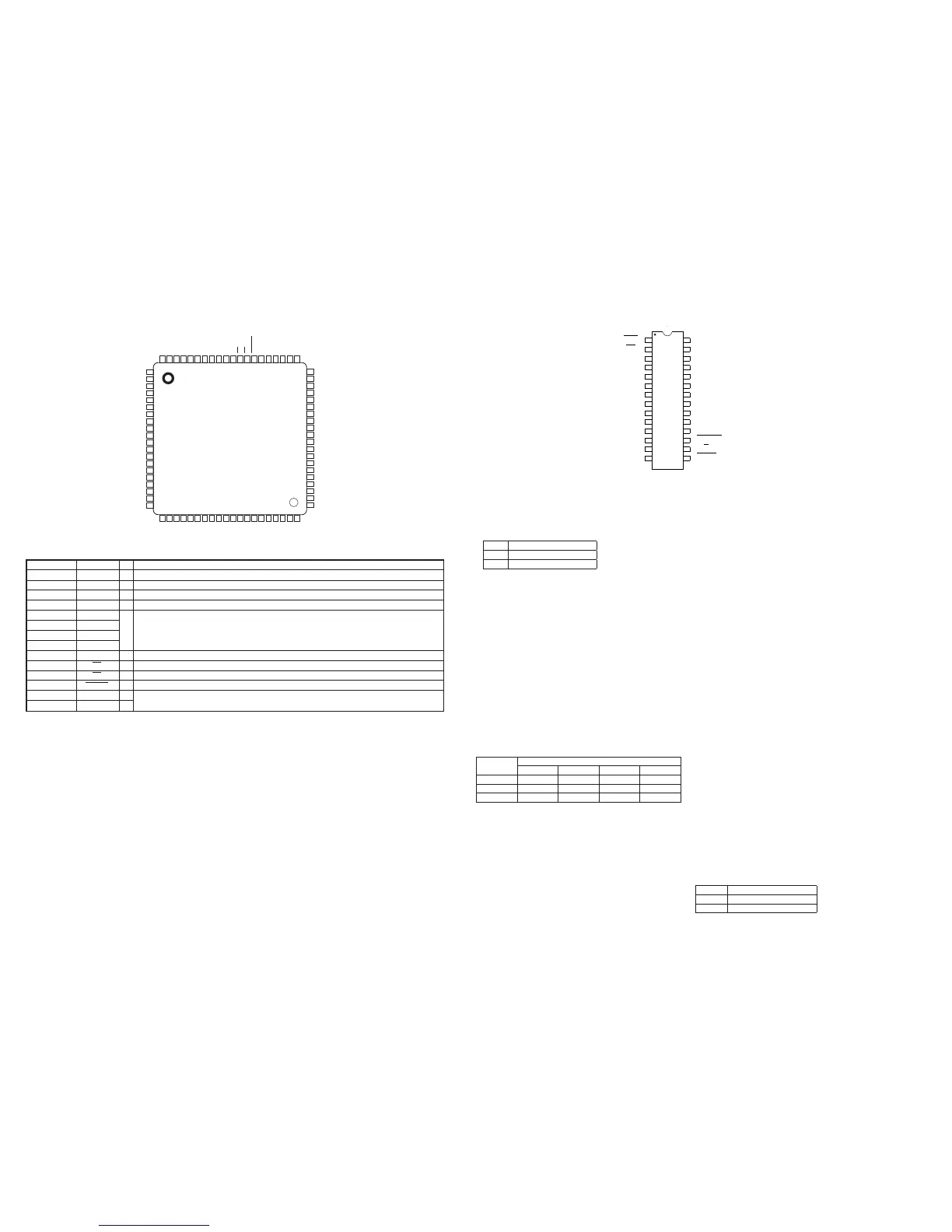
QY01 : ML9207-01
3~37 SEG1~35 O FL display anode drive output pin
39~62 COM1~24 O FL display grid drive output pin
1,2, 79, 80 AD1~4 O FL display anode drive output pin
72~75 P1~4 O General port output pin
71 VDD
VDD-GND: Power supply for logic block
38, 78 VDISP1~2
VDISP-VFL: Power supply for FL display drive
64 GND
For V
DD and VDISP, apply from same power source
63, 76 VFL1~2
70 DA I Serial data input pin (positive logic)
69 CP I Shift clock input pin
68 CS I Chip select input pin
67 RESET I Reset input pin
65 OSC0 I
Pin for self-oscillation
66 OSC1 O
Pin Name FunctionPin No. I/O
ML9207-01 Terminal Function
61
62
63
64
65
66
67
68
69
70
71
72
73
74
75
76
77
78
79
80
COM23
COM24
V
FL1
GND
OSC0
OSC1
RESET
CS
CP
DA
V
DD
P1
P2
P3
P4
V
FL2
NC
V
DISP2
AD1
AD2
1
2
3
4
5
6
7
8
9
10
11
12
13
14
15
16
17
18
19
20
AD3
AD4
SEG1
SEG2
SEG3
SEG4
SEG5
SEG6
SEG7
SEG8
SEG9
SEG10
SEG11
SEG12
SEG13
SEG14
SEG15
SEG16
SEG17
SEG18
40
39
38
37
36
35
34
33
32
31
30
29
28
27
26
25
24
23
22
21
COM2
COM1
V
DISP1
SEG35
SEG34
SEG33
SEG32
SEG31
SEG30
SEG29
SEG28
SEG27
SEG26
SEG25
SEG24
SEG23
SEG22
SEG21
SEG20
SEG19
60
59
58
57
56
55
54
53
52
51
50
49
48
47
46
45
44
43
42
41
COM22
COM21
COM20
COM19
COM18
COM17
COM16
COM15
COM14
COM13
COM12
COM11
COM10
COM9
COM8
COM7
COM6
COM5
COM4
COM3
10. MICROPROCESSOR AND IC DATA
QD61 : CS4397
Reset - RST
Pin 1, Input
Function:
The device enters a low power mode and all internal state
machines registers are reset when low. When
high, the device will be in a normal operation mode .
RST DESCRIPTION
0 Enabled
1 Normal operation mode
Digital Ground - DGND
Pins 6 and 9, Inputs
Function:
Digital ground reference.
Digital Power - VD
Pins 7 and 8, Input
Function:
Digital power supply. Typically 5.0 to 3.0 VDC.
Master Clock - MCLK
Pin 10, Input
Function:
The master clock frequency must be either 256x, 384x, 512x or
768x the input sample rate in Single
Speed Mode; either 128x, 192x 256x or 384x the input sample
rate in Double Speed Mode; or 64x, 96x
128x or 192x the input sample rate in Quad Speed Mode. Tables
4-6 illustrate the standard audio sample
rates and the required master clock frequencies.
Sample
Rate (kHz)
MCLK (MHz)
256x 384x 512x 768x
32 8.1920 12.2880 16.3840 24.5760
44.1 11.2896 16.9344 22.5792 33.8688
48 12.2880 18.4320 24.5760 36.8640
Table 4. Single Speed (16 to 50 kHz sample rates) Common Clock
Frequencies
Serial Clock - SCLK
Pin 11, Input
Function:
Clocks individual bits of serial data into the SDATA pin. The
required relationship between the Left/Right
clock, serial clock and serial data is defi ned by either the Mode
Control Byte in Control Port Mode or the
M0 - M4 pins in Hardware Mode. The options are detailed in
Figures 29-33
Left/Right Clock - LRCK
Pin 12, Input
Function:
The Left/Right clock determines which channel is currently being
input on the serial audio data input,
SDATA. The frequency of the Left/Right clock must be at the input
sample rate. Audio samples in
Left/Right sample pairs will be simultaneously output from the
digital-to-analog converter whereas
Right/Left pairs will exhibit a one sample period difference. The
required relationship between the
Left/Right clock, serial clock and serial data is defi ned by the
Mode Control Byte and the options are de-
tailed in Figures 29-33
Serial Audio Data - SDATA
Pin 13, Input
Function:
Serial audio data is input on this pin. The selection of the Digital
Interface Format is determined by set-
tings of the Mode select as detailed in Figures 29-33. The data is
clocked into SDATA via the serial clock
and the channel is determined by the Left/Right clock. The
required relationship between the Left/Right
clock, serial clock and serial data is defi ned by the Mode Control
Byte and the options are detailed inin
Figures 29-33
Soft Mute - MUTE
Pin 15, Input
Function:
The analog outputs will ramp to a muted state when enabled. The
ramp requires 1152 left/right clock cy-
cles in Single Speed, 2304 cycles in Double Speed and 4608
cycles in Quad Speed mode. The bias volt-
age on the outputs will be retained and MUTEC will go active at
the completion of the ramp period.
The analog outputs will ramp to a normal state when this function
transitions from the enabled to disabled
state. The ramp requires 1152 left/right clock cycles in Single
Speed, 2304 cycles in Double Speed and
4608 cycles in Quad Speed mode. The MUTEC will release
immediately on setting MUTE = 1.
The converter analog outputs will mute when enabled. The bias
voltage on the outputs will be retained
and MUTEC will go active during the mute period.
Mute DESCRIPTION
0 Enabled
1 Normal operation mode
PCM MODE
1
2
3
4
5
6
7
8
9
10
11
12
5
1
2
6
28
27
26
25
24
23
22
21
20
19
18
17
13
14
16
15
Reset RST
VREF Voltage Reference
See Description M4(AD0/CS
) FILT+ Reference Filter
See Description M3(AD1/CDIN) FILT- Reference Ground
See Description M2(SCL/CCLK) CMOUT Common ModeS Voltage
See Description M0(SDA/CDOUT) AOUTL- Differential Output
Digital Ground DGND AOUTL+ Differential Output
Digital Power VD VA Analog Power
Digital Power VD AGND Analog Ground
Digital Ground DGND AOUTR+ Differential Output
Master Clock MCLK AOUTR- Differential Output
Serial Clock SCLK AGND Analog Ground
Left/Right Clock LRCK MUTEC
Mute Control
Serial Data SDATA C/H
Control port/Hardware select
See Description M1 MUTE
Soft Mute
 Loading...