48
IC715:AK5380
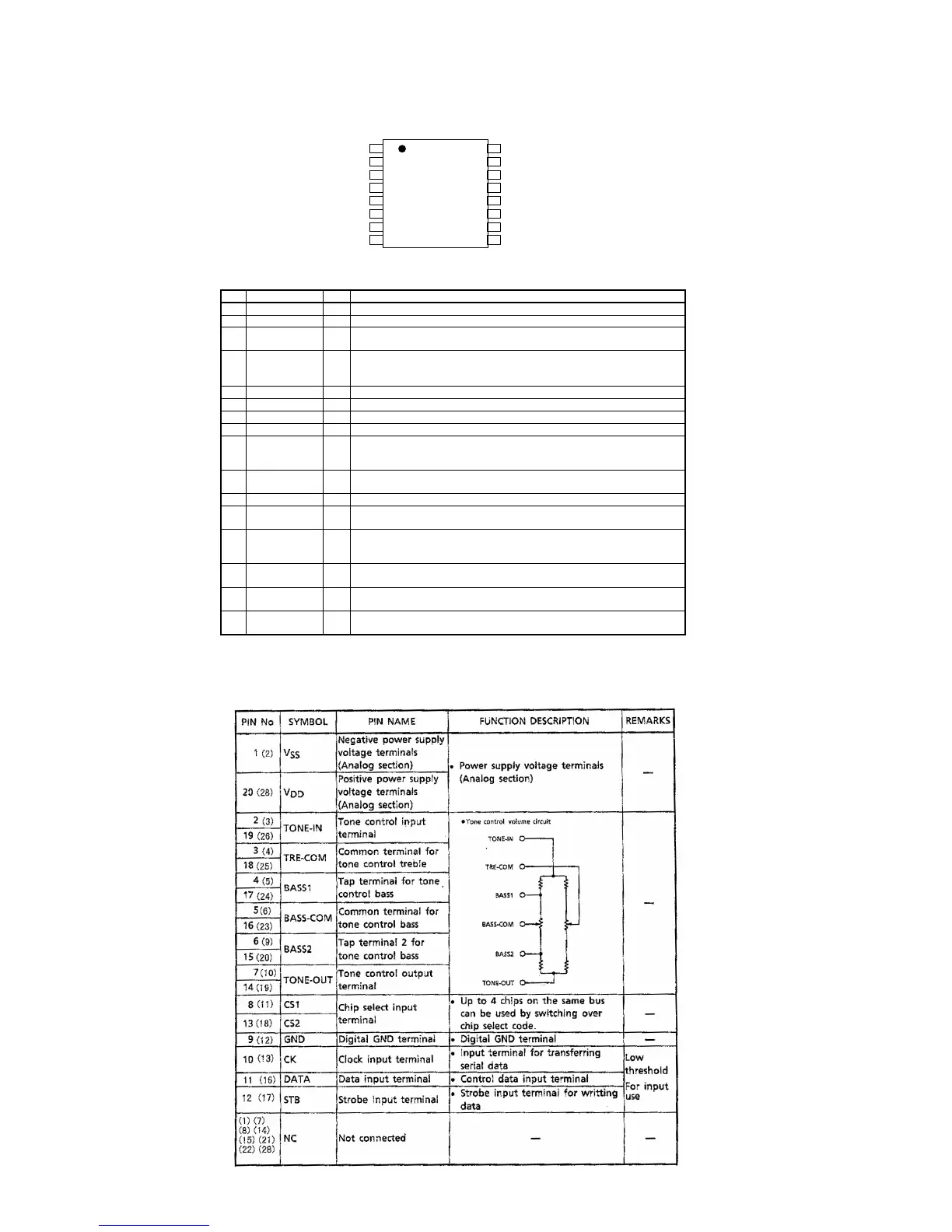
6. IC DATA
No. Pin Name I/O Description
1 AINR I Rch Analog Input Pin
2 AINL I Lch Analog Input Pin
3 NC - NC Pin
No internal bonding.
4 VCOM O Common Voltage Output Pin
Normally connected to AGND with a 0.1 F ceramic capacitor in parallel with an
electrolytic capacitor less than 2.2 F.
5 AGND - Analog Ground Pin, 0V
6VA -
Analog Power Supply Pin, +4.5 +5.5V
7VD -
Digital P ower Supply Pin, +2.7 +5.5V(fs=48kHz), +4.5 +5.5V(fs=96kHz)
8 DGND - Digital Ground Pin, 0V
9 SDTO O Serial Data Output Pin
Data bits are presented MSB first, in 2’s complement format.
This pin is “L ” in the power-down mode.
10 LRCK I Left/Right Channel Select Pin
The fs clock is input to this pin.
11 MCLK I Master Clock Input Pin
12
SCLK I Serial Data Input Pin
Output data is clocked out on the falling edge of SCLK.
13 PDN I Power-Down Pin
When “L ”, the circuit is in power-down mode.
The AK5380 should always be reset upon power-up.
14 DIF I Serial Interface Format Pin
“L ”: MSB justified, “H”: I
2
S
15 TTL I Digital Input Level Select Pin
“L ”: CMOS level (VD=2.7 5.5V), “H”: TTL level (VD=4.5 5.5V)
16 TST I Test Pin (Internal pull-down pin)
This pin should be left open.
1
AINR
AINL
VCOM
NC
AGND
VA
VD
DGND
Top
View
2
3
4
5
6
7
8
TST
TTL
PDN
DIF
SCLK
MCLK
LRCK
SDTO
16
15
14
13
12
11
10
9
Pin Assignment
Pin Function
IC504:TC9481
Pin Function