2006-2019 Microchip Technology Inc. DS30009711C-page 19
I/O Ports with PPS
5.0 PORT DESCRIPTIONS
Refer to the specific device data sheet for a description of the available I/O ports, peripheral
multiplexing details and available Peripheral Pin Select pins.
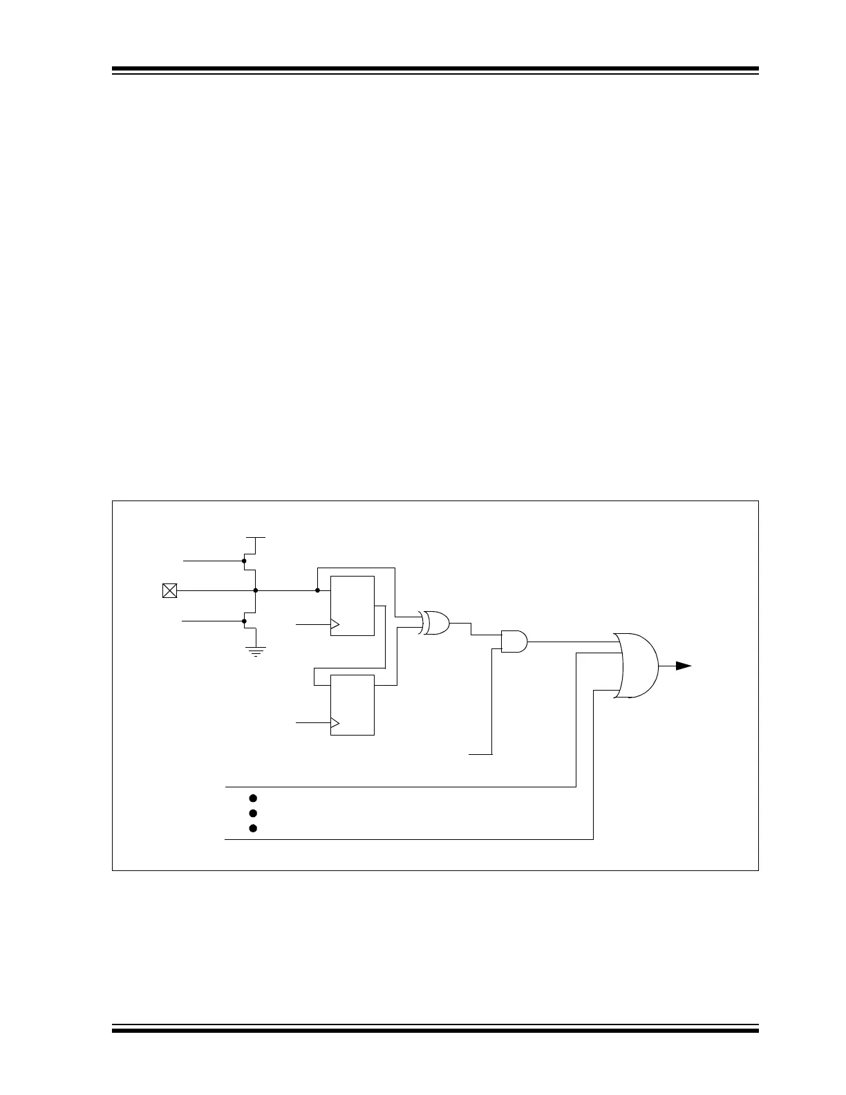
6.0 CHANGE NOTIFICATION (CN) PINS
The Change Notification (CN) pins provide dsPIC33/PIC24 devices the ability to generate inter-
rupt requests to the processor in response to a Change-of-State (COS) on selected input pins.
The total number of available CN inputs is dependent on the selected dsPIC33/PIC24 device.
Refer to the specific device data sheet for further details.
Figure 6-1 shows the basic function of the CN hardware.
6.1 CN Control Registers
There are four control registers associated with the CN module. The CNENx registers contain
the CNxIE control bits, where ‘x’ denotes the number of the CN input pin. The CNxIE bit must be
set for a CN input pin to interrupt the CPU.
The CNPUx/CNPDx registers contain the CNxPUE/CNxPDE control bits. Each CN pin has a
weak pull-up/pull-down device connected to the pin, which can be enabled or disabled using the
CNxPUE/CNxPDE control bits. The weak pull-up/pull-down devices act as a current source/sink
that is connected to the pin and eliminate the need for external resistors when push button or
keypad devices are connected. Refer to the “Electrical Characteristics” section of the specific
device data sheet for CN pull-up/pull-down device current specifications.
Figure 6-1: Input Change Notification Block Diagram
CN
DQ
C
CN0IE (CNEN1<0>)
CN0
Pin
CN0PUE
(CNPU1<0>)
CN0 Change
CN1 Change
CNx Change
Interrupt
CN1-CNx
(details not
shown)
CN0PDE
(CNPD1<0>)
VDD
DQ
C