2006-2019 Microchip Technology Inc. DS30009711C-page 21
I/O Ports with PPS
7.0 REGISTER MAPS
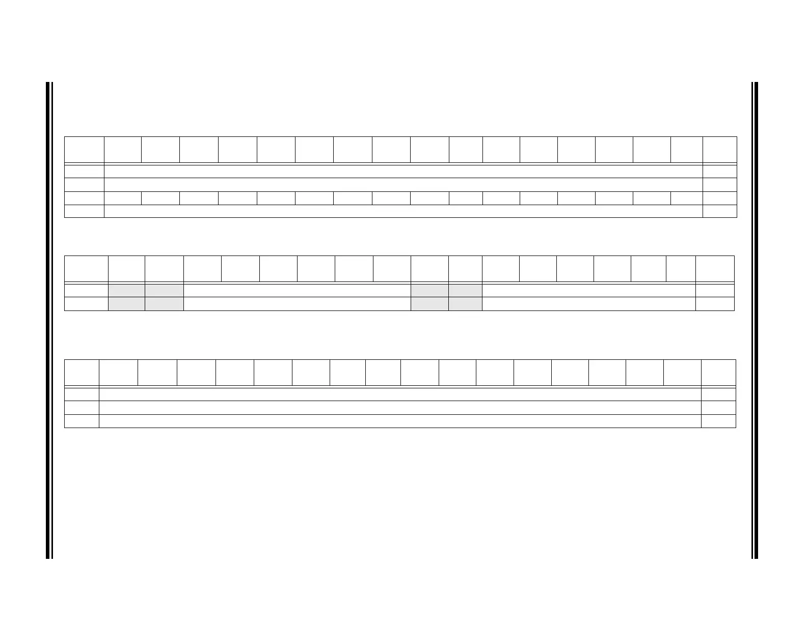
A summary of the registers associated with the dsPIC33/PIC24 I/O ports is provided in Tabl e 7- 1, Table 7-2 and Table 7 -3 .
Table 7-1: Special Function Registers Associated with I/O Ports
(1)
Table 7-2: Special Function Registers Associated with Peripheral Pin Selection
(1)
Table 7-3: Special Function Registers Associated with Change Notification Pins
(1)
Name Bit 15 Bit 14 Bit 13 Bit 12 Bit 11 Bit 10 Bit 9 Bit 8 Bit 7 Bit 6 Bit 5 Bit 4 Bit 3 Bit 2 Bit 1 Bit 0
All
Resets
TRISx PORTx Data Direction Control bits FFFF
LATx PORTx Data Latch bits xxxx
PORTx Rx15 Rx14 Rx13 Rx12 Rx11 Rx10 Rx9 Rx8 Rx7 Rx6 Rx5 Rx4 Rx3 Rx2 Rx1 Rx0 xxxx
ODCx PORTx Open-Drain Control bits 0000
Note 1: Refer to the specific device data sheet for the I/O Ports register map details.
Name Bit 15 Bit 14 Bit 13 Bit 12 Bit 11 Bit 10 Bit 9 Bit 8 Bit 7 Bit 6 Bit 5 Bit 4 Bit 3 Bit 2 Bit 1 Bit 0
All
Resets
RPINRx
— — Input Function bits<5:0> — — Input Function bits<5:0> 3F3F
(2)
RPORy — — RPnR<5:0> — —RPnR<5:0>0000
Note 1: Refer to the specific device data sheet for Peripheral Pin Select register map details.
2: The number of bits implemented varies with the number of pins the device has.
Name Bit 15 Bit 14 Bit 13 Bit 12 Bit 11 Bit 10 Bit 9 Bit 8 Bit 7 Bit 6 Bit 5 Bit 4 Bit 3 Bit 2 Bit 1 Bit 0
All
Resets
CNENx Change Notification Interrupt Enable bits 0000
CNPUx Change Notification Pull-up Enable bits 0000
CNPDx Change Notification Pull-Down Enable bits 0000
Note 1: Refer to the specific device data sheet for Change Notification Pin register details.