dsPIC33/PIC24 Family Reference Manual
DS30009740B-page 22 2010-2013 Microchip Technology Inc.
7.0 SEGMENT ENABLES
The LCDSEx registers are used to select the pin function for each segment pin. The selection
allows each pin to operate as either an LCD segment driver or a digital only pin. To configure the
pin as a segment driver, the corresponding bits in the LCDSEx registers must be set to ‘1’.
If the pin is a digital I/O, the corresponding TRIS bit controls the data direction. Any bit set in the
LCDSEx registers overrides any bit settings in the corresponding TRIS register.
8.0 PIXEL CONTROL
The LCDDATAx registers contain bits that define the state of each pixel. Each bit defines one
unique pixel. Tab le 3-2 shows the correlation of each bit in the LCDDATAx registers to the
respective common and segment signals.
Any LCD pixel location not being used for display can be used as general purpose RAM.
9.0 LCD FRAME FREQUENCY
The rate at which the COM and SEG outputs change is called the LCD frame frequency.
10.0 LCD WAVEFORM GENERATION
LCD waveform generation is based on the philosophy that the net AC voltage across the dark
pixel should be maximized and the net AC voltage across the clear pixel should be minimized.
The net DC voltage across any pixel should be zero.
The COM signal represents the time slice for each common, while the SEG contains the pixel data.
The pixel signal (COM-SEG) will have no DC component and can take only one of the two RMS
values. The higher RMS value will create a dark pixel and a lower RMS value will create a clear
pixel.
As the number of commons increases, the delta between the two RMS values decreases. The
delta represents the maximum contrast that the display can have.
The LCDs can be driven by two types of waveforms: Type-A and Type-B. In a Type-A waveform,
the phase changes within each common type, whereas a Type-B waveform’s phase changes on
each frame boundary. Thus, Type-A waveforms maintain 0 V
DC over a single frame, whereas
Type-B waveforms take two frames.
Note: On a Power-on Reset, these pins are configured as digital I/O.
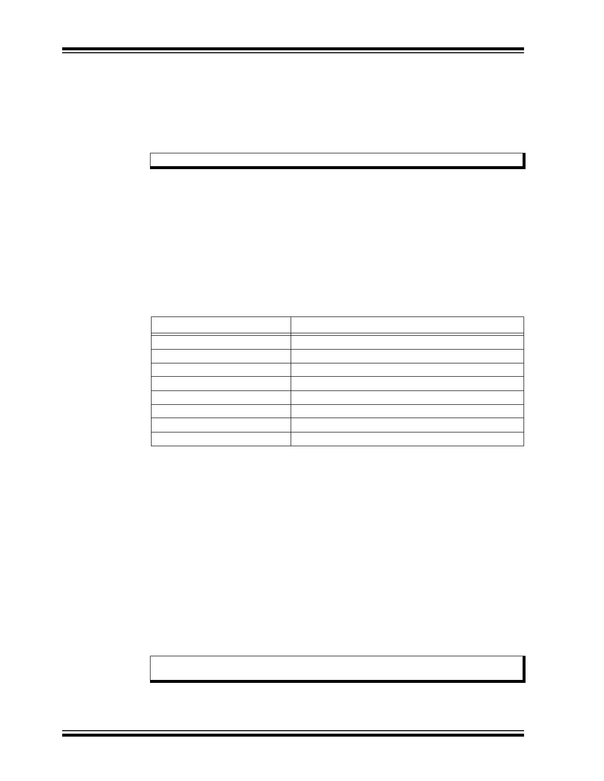
Table 9-1: Frame Frequency Formulas
Multiplex Frame Frequency =
Static (000) Clock Source/(4 x 1 x (LP<3:0> + 1))
1/2 (001) Clock Source/(2 x 2 x (LP<3:0> + 1))
1/3 (010) Clock Source/(1 x 3 x (LP<3:0> + 1))
1/4 (011) Clock Source/(1 x 4 x (LP<3:0> + 1))
1/5 (100) Clock Source/(1 x 5 x (LP<3:0> + 1))
1/6 (101) Clock Source/(1 x 6 x (LP<3:0> + 1))
1/7 (110) Clock Source/(1 x 7 x (LP<3:0> + 1))
1/8 (111) Clock Source/(1 x 8 x (LP<3:0> + 1))
Note: The clock source is FRC/8192, SOSC/32 or LPRC/32.
Note: If Sleep has to be executed with LCD Sleep enabled (SLPEN (LCDCON<6>) = 1),
care must be taken to execute Sleep only when the V
DC on all the pixels is ‘0’.