dsPIC33/PIC24 Family Reference Manual
DS30009740B-page 6 2010-2013 Microchip Technology Inc.
3.0 LCD SEGMENT PINS CONFIGURATION
The LCDSEx registers configure the functions of the port pins. Setting the segment enable bit for
a particular segment configures that pin as an LCD driver. There are four LCD Segment Enable
registers, as shown in Table 3-1. The prototype LCDSEx register is shown in Register 3-1.
Once the module is initialized for the LCD panel, the individual bits of the LCDDATAx registers
are cleared, or set, to represent a clear or dark pixel, respectively.
Specific sets of LCDDATAx registers are used with specific segments and common signals. Each
bit represents a unique combination of a specific segment connected to a specific common.
Individual LCDDATAx bits are named by the convention, “SxxCy”, with “xx” as the segment
number and “y” as the common number. The relationship is summarized in Register 2-2. The
prototype LCDDATAx register is shown in Register 3-2.
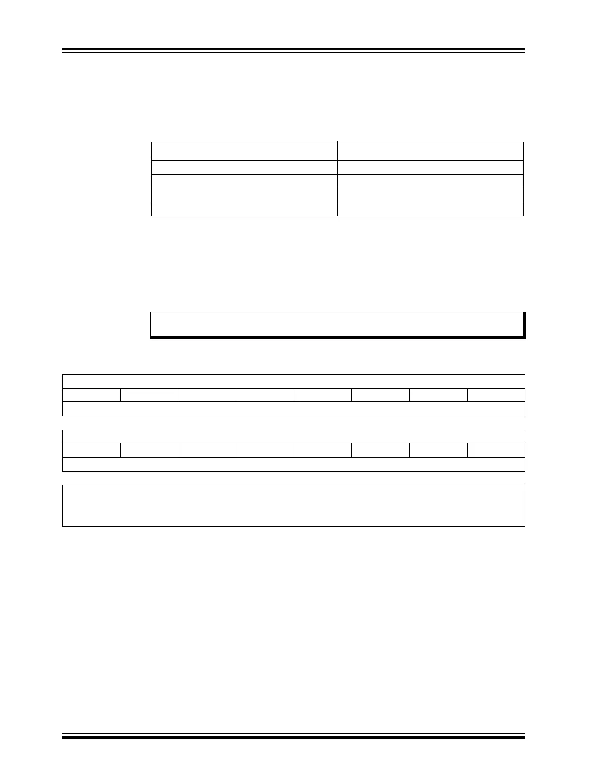
Register 3-1: LCDSEx: LCD Segment x Enable Register
Table 3-1: LCDSEx Registers and Associated Segments
Register Segments
LCDSE0 Seg 15:Seg 0
LCDSE1 Seg 31:Seg 16
LCDSE2 Seg 47:Seg 32
LCDSE3 Seg 63:Seg 48
Note: Not all LCDSEx and LCDDATAx registers are implemented in all devices. Refer to
the specific device data sheet for more details.
R/W-0 R/W-0 R/W-0 R/W-0 R/W-0 R/W-0 R/W-0 R/W-0
SE(n+15) SE(n+14) SE(n+13) SE(n+12) SE(n+11) SE(n+10) SE(n+9) SE(n+8)
bit 15 bit 8
R/W-0 R/W-0 R/W-0 R/W-0 R/W-0 R/W-0 R/W-0 R/W-0
SE(n+7) SE(n+6) SE(n+5) SE(n+4) SE(n+3) SE(n+2) SE(n+1) SE(n)
bit 7 bit 0
Legend:
R = Readable bit W = Writable bit U = Unimplemented bit, read as ‘0’
-n = Value at POR ‘1’ = Bit is set ‘0’ = Bit is cleared x = Bit is unknown
bit 7-0 SE(n + 15):SE(n): Segment Enable bits
For LCDSE0: n = 0
For LCDSE1: n = 16
For LCDSE2: n = 32
For LCDSE3: n = 48
1 = Segment function of the pin is enabled; digital I/O is disabled
0 = Segment function of the pin is disabled