B
RX-_U1
TX+_U1
TX-_U1
RX+_U1
CMT
RX+_U1
RX-_U1
TX+_U1
TX-_U1
TX+_U1
RX-_U1
TX-_U1
RX+_U1
RXP_U1
RXM_U1
CT_RX1
CT_TX1
CMR
TX_P_U1
RX-_U1
RX+_U1
TX-_U1
TX+_U1
TXP_U1
TXM_U1
RX_M_U1
RX_P_U1
TX_M_U1
CT_TX1
CT_RX1
U1_CHASSIS_GND
EXT_GNDU1_CHASSIS_GND
TXP_U1 (3)
RXP_U1 (3)
TXM_U1 (3)
RXM_U1 (3)
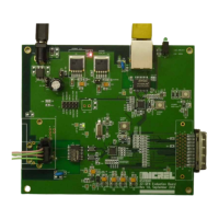
Component placement for this schematic page
will allow for flow thru routing of TX and RX
differential pairs on top PCB layer.
Three connector options are provided.
Only one may be mounted at a time.
The footprints are closely spaced so as to minimize trace stubs.
R58 and R96:
Place one near J1/J2/J3
Place the other nearer L1
These components are optional. They are suggested
only for applications requiring maximum noise immunity.
J2
MQS 4 Pos TE 1379165-1
J2
MQS 4 Pos TE 1379165-1
1
2
3
4
C92
opt
C92
opt
R96 optR96 opt
R59 0R59 0
C16
1uF
C16
1uF
R52 75R52 75
T1
TDK TLA-8T104WLF
T1
TDK TLA-8T104WLF
1
2
3
6
8
7
16
15
14
11
10
9
R50 75R50 75
C93
opt
C93
opt
C94
opt
C94
opt
R32
opt
R32
opt
R49 75R49 75
C90
opt
C90
opt
J1
RJ-45 Jack
J1
RJ-45 Jack
8
7
6
5
4
3
2
1
TH1
TH2
C17
1000pF / 2kV
C17
1000pF / 2kV
R34
opt
R34
opt
R58 optR58 opt
C91
opt
C91
opt
C18
1uF
C18
1uF
L2
TDK ACT45
L2
TDK ACT45
1
2
4
3
L3
TDK ACT45
L3
TDK ACT45
1
2
4
3
R48 75R48 75
516
61
J3
Sumitomo 6098-6793
516
61
J3
Sumitomo 6098-6793
1
1
2
2
3
3
4
4
5
5
6
6
7
7
8
8
9
9
10
10
11
11
12
12
13
13
14
14
15
15
16
16