-
272
-
Precautions for Safety
・
Since the following precaution is the important contents for safety, be sure to observe them.
WARNING and CAUTION are described as follows:
! WARNING Indicates an imminently hazardous situation which will result in death or serious
injury if proper safety procedures and instructions are not adhered to.
! CAUTION Indicates a potentially hazardous situation which may result in minor or moderate
injury if proper safety procedures and instructions are not adhered to.
! WARNING
・ Securely exchange the
PCB
according to this procedure.
If the PCB is incorrectly exchanged, it will cause an electric shock or fire.
・ Be sure to check that the power source for the outdoor unit is turned OFF before exchanging the PCB.
The PCB exchange under current-carrying will cause an electric shock or fire.
・ After finishing the PCB exchange, check that wiring is correctly connected with the PCB before
power distribution. If the PCB is incorrectly exchanged, it will cause an electric shock or fire.
! CAUTION
・ Band the wiring so as not to tense because it will cause an electric shock.
Exchange the inverter PCB according to the following procedure.
1. Disassembly
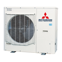
1.1 After the breaker is shut down, remove the service panel and top panel. (Refer to Fig.1).
1.2 Don't touch the controller until three minutes have passed after the breaker is shut down.
(After having shut down the breaker, some capacitor is held by high voltage. It is very dangerous
to touch the controller in this condition.) Confirm the voltage (DC) is under 30 V with the harnesses
connected to control PCB. (Refer to Fig.2)
1.3 Unlock the band (1 place) and disconnect the connectors and round terminals from the user side of terminal
blo
ck
and control PCB as shown in (A) in Fig.2.
1.4 Insert the CNP1 connector to the grommet of control panel. (Refer to Fig.2)
1.5 Cut the band as shown in (B) in Fig.2, and remove
the white wiring from CT1.
1.6 Cut the bands (4 places), while disconnect the CNLA connector and the faston terminals (“P” and “N2”)
as shown in (C) in Fig.3.
1.7 Remove the screws of the electr
olytic capacitor as shown in Fig.3.
1.8 Remove the screws (8 places) as shown in Fig.4, and remove the control panel from nail-part in left-side
with pulling up. Next, disconnect CNI
2 and CNI4, and remove the control panel from controller.
After elapsing 3 minutes
from power OFF
*Presence and shape of electric component
may vary according to model.
CNQ1
CNN1
CNR1
CNFAN1
CNEEV2
CNEEV1
CNL2
CNL1
CNP1
CNF2
CNTH
Insert the CNP1 connector to the grommet
(A)
Confirm the voltage (DC) is under 30 V
between No.1 and No.3 on CNA1
Fig.2 Parts arrangement view of controller and
voltage measurement points
Fig.3 Top view of controller
Fig.4 Removing procedure of control panel
1st. Remove the screws (8 places)
Control panel
CNI2
CNI4
Control panel
Inverter PCB
4th. Remove the control panel from controller
(B)
Control PCB
N.F. PCB
Band
White wiring
CT1
TB6
CNLA
Cut the band and remove
white wiring from CT1
2nd. Pull up the control panel and pull
towards oneself
3rd.
Disconnect the
connectors
Nail-part
Cut the bands (4 places)
Disconnect CNLA
A.F. module
Fig.1 Outdoor unit overall view
Remove
(Top panel)
Remove
(Service panel)
N2
P
(C)
Electrolytic capacitor (C1)
Remove the screws
Disconnect the faston terminals
CN
P1
CNF1
Terminal block (User side)
Unlock the band
Connectors are not
half inserted
Parts Ref.No Sequence Position
1 A
2 B
3 A
4 B
Inverter PCB TB1-11 - - 2.0
~
2.4 N
・
m
N.F. PCB TB6 - - 1.2
~
1.4 N
・
m
L,N,E,E(SL) - - 1.2
~
1.4 N
・
m
A1,A2,B1,B2 - - 1.2
~
1.4 N
・
m
Electrolytic capacitor C1 - - 2.5
~
2.7 N
・
m
Tightening torque
Initial
Final
-
-
-
-
-
Terminal block
IPM IC2
0.2
~
0.44 N
・
m
1.2
~
1.4 N
・
m
2. Exchange
2.1 Remove the screw from support panel and rotate the support panel to counterclockwise direction as shown in Fig.5.
(By doing so, you can see the locking spacer of the inverter PCB.)
2.2 Disconnect the connectors and round terminals, and remove the screws on the IPM (IC2) as shown in (D) in Fig.6.
2.3 Remove the inverter PCB.
2.4 Wipe off the silicone grease neatly on the heat sink.
2.5 Match the setting of new PCB switches (JSW10, 11) with former PCB. (Refer to Fig.6)
2.6 Paste a bundled silic
one grease uniformly on the radiating surface of the IPM (IC2) on the new PCB, and attach
the new PCB.
Without silicone grease pasting or its irregularities in the surface may damage to the inverter PCB.
(One-third to a half of the grease tube is adequate volume.)
2.7 Tighten the screws of IPM (IC2) on new PCB (Refer to table for recommended tightening torque), and
reconnect the connectors and round terminals as before. (Confirm that the connectors are not half inserted.)
3. Installation
3.1 Return the support panel to original position and tighten with the screw as before.
3.2 Install the control panel to nail-part on controller as shown in fig.7. And, pull out the CNP1 connector to
control PCB side from the grommet after
bundle the wiring to clamp as shown in fig.7.
3.3 Tighten the screws of electrolytic capacitor as shown Fig.8. (Refer to table for recommended tightening torque)
3.4 Reconnect the CNLA connector, and faston terminals to A.F. module (“P” and “N2”) as before.
3.5 Pass the white wiring through CT1 on the control PCB (Refer to Fig.7), and tighten the screw of TB6 in the N.F. PCB
as before. (Refer to table for recommended tightening torque)
Using bands in the package, bundle the wiring at cutting point on 1.4 and 1.5 as before. (Refer to Fig.3 and Fig.7)
3.6 Tighten the screws (8 places) as shown in Fig.4 as before.
3.7 Reconnect the connectors and round terminals to control PCB and the user side of terminal block as before.
(Confirm the connectors are not half inserted.) (Refer to table for
recommended tightening torque)
Table recommended tightening torque
TB10
TB3
TB4
TB11
CNCAN
CNI2 **
CNACT1
CNI4 **
CNO
TB1
TB2
IC2
TB6
TB5
**TB9
**TB8
**TB7
JSW11
Parts No.
JSW10
Screw
Rotate
Support panel
Ⓐ Ⓑ
Inverter PCB
Support panel
A.F. module
IPM (IC2)
Fig.7 Installing procedure of control panel
Fig.6 Parts arrangement view of inverter PCB
Fig.5 Inverter side view of controller
Pass through the white wiring in
the direction of arrow.
Nail-part
Grommet
(D)
(D)
*Presence and shape of electric component
may vary according to model.
Fig.8 Installing procedure of electrolytic capacitor
To “P” (A.F. module)
CNA1, 2 (Control PCB)
To TB5 (Inverter PCB)
To TB6 (Inverter PCB)
To “N2” (A.F. module)
CNA1, 2 (Control PCB)
Electrolytic capacitor (C1)
Band
White wiring
CT1
TB6
CNLA
Bundle the white wiring as before.
Back side view
Clamp
To CNP1
Grommet
Electrolytic capacitor (C1)
Bundle the CNP1 wiring as before.
Connectors are not
half inserted
** These connectors and round terminals
are disconnected in 1.8.
 Loading...
