6 Chapter 1. Introduction
1.1.1 Input stage
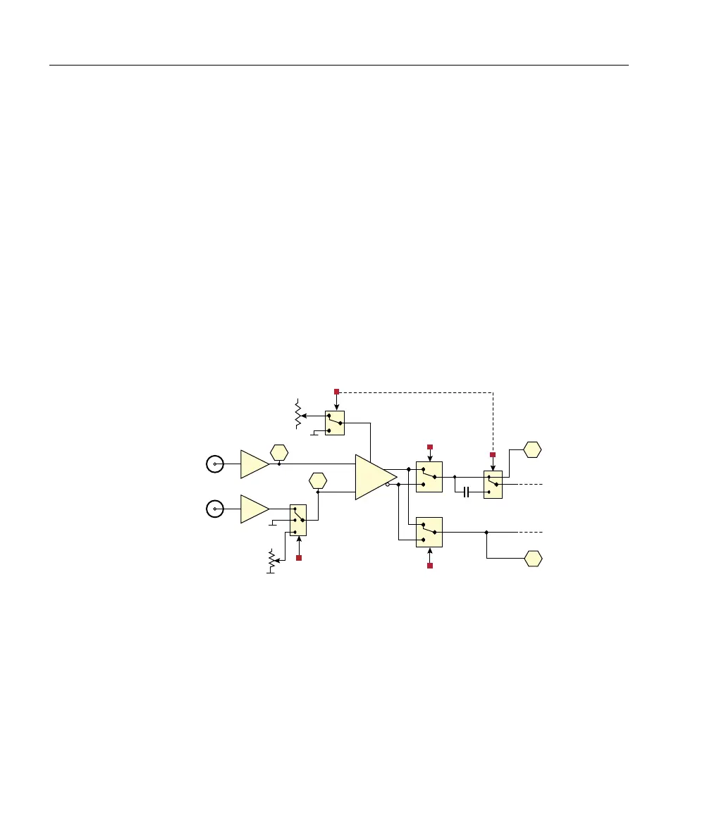
The input stage of the FSC (figure 1.5) generates an error signal as
V
ERR
= V
A
− V
B
− V
OFFSET
. V
A
is taken from the “A IN” SMA con-
nector, and V
B
is set using the CHB selector switch, which chooses
between the “B IN” SMA connector, V
B
= 0 or V
B
= V
REF
as set by
the adjacent trimpot.
The controller acts to servo the error signal towards zero, which
defines the lock point. Some applications may benefit from small
adjustments to the DC level to adjust this lock point, which can be
achieved with the 10-turn knob ERR OFFSET for up to ±0.1 V shift,
provided the INPUT selector is set to “offset” mode (∆). Larger offsets
can be achieved with the REF trimpot.
B IN
0v
+
–
CHB
+
+
–
V
REF
A IN
ERR OFFSET
FAST SIGN
SLOW SIGN
INPUT
FE
SE
SLOW ERR
Fast error
Slow error
FAST ERR
DC block
0v
0v
INPUT
B
A
Figure 1.5: Schematic of the FSC input stage, showing coupling, offset
and polarity controls. Hexagons are monitored signals available via the
front-panel selector switches.


 To Next Page