MC9S12DT256 Device User Guide — V03.07
119
A.7 SPI
This section provides electrical parametrics and ratings for the SPI.
In Table A-18 the measurement conditions are listed.
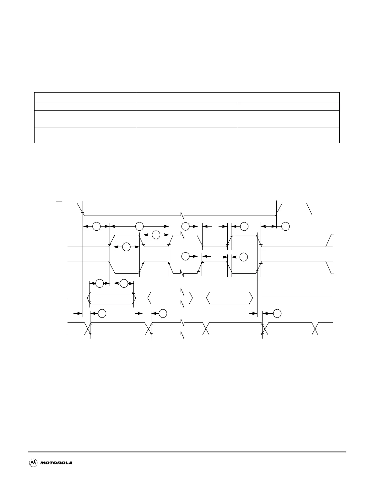
A.7.1 Master Mode
In Figure A-6 the timing diagram for master mode with transmission format CPHA=0 is depicted.
Figure A-6 SPI Master Timing (CPHA=0)
In Figure A-7 the timing diagram for master mode with transmission format CPHA=1 is depicted.
Table A-18 Measurement Conditions
Description Value Unit
Drive mode full drive mode —
Load capacitance C
LOAD,
on all outputs
50 pF
Thresholds for delay
measurement points
(20% / 80%) VDDX V
SCK
(OUTPUT)
SCK
(OUTPUT)
MISO
(INPUT)
MOSI
(OUTPUT)
SS
1
(OUTPUT)
1
9
5 6
MSB IN
2
BIT 6 . . . 1
LSB IN
MSB OUT
2
LSB OUT
BIT 6 . . . 1
11
4
4
2
10
(CPOL = 0)
(CPOL = 1)
3
13
13
1.if configured as an output.
2. LSBF = 0. For LSBF = 1, bit order is LSB, bit 1, ..., bit 6, MSB.
12
12
 Loading...