MC9S12DT256 Device User Guide — V03.07
91
A.1.4 Current Injection
Power supply must maintain regulation within operating V
DD5
or V
DD
range during instantaneous and
operating maximum current conditions. If positive injection current (V
in
>V
DD5
) is greater than I
DD5
, the
injection current may flow out of VDD5 and could result in external power supply going out of regulation.
Ensure external VDD5 load will shunt current greater than maximum injection current. This will be the
greatest risk when the MCU is not consuming power; e.g. if no system clock is present, or if clock rate is
very low which would reduce overall power consumption.
A.1.5 Absolute Maximum Ratings
Absolute maximum ratings are stress ratings only. A functional operation under or outside those maxima
is not guaranteed. Stress beyond those limits may affect the reliability or cause permanent damage of the
device.
This device contains circuitry protecting against damage due to high static voltage or electrical fields;
however, it is advised that normal precautions be taken to avoid application of any voltages higher than
maximum-rated voltages to this high-impedance circuit. Reliability of operation is enhanced if unused
inputs are tied to an appropriate logic voltage level (e.g., either V
SS5
or V
DD5
).
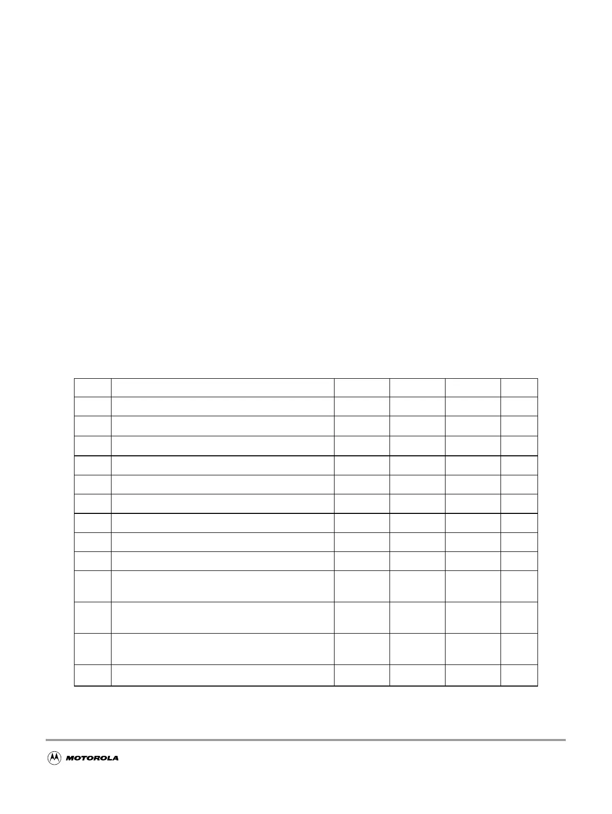
Table A-1 Absolute Maximum Ratings
1
NOTES:
1. Beyond absolute maximum ratings device might be damaged.
Num Rating Symbol Min Max Unit
1 I/O, Regulator and Analog Supply Voltage
V
DD5
-0.3 6.0 V
2
Digital Logic Supply Voltage
2
V
DD
-0.3 3.0 V
3
PLL Supply Voltage
2
V
DDPLL
-0.3 3.0 V
4 Voltage difference VDDX to VDDR and VDDA
∆
VDDX
-0.3 0.3 V
5 Voltage difference VSSX to VSSR and VSSA
∆
VSSX
-0.3 0.3 V
6 Digital I/O Input Voltage
V
IN
-0.3 6.0 V
7 Analog Reference
V
RH,
V
RL
-0.3 6.0 V
8 XFC, EXTAL, XTAL inputs
V
ILV
-0.3 3.0 V
9 TEST input
V
TEST
-0.3 10.0 V
10
Instantaneous Maximum Current
Single pin limit for all digital I/O pins
3
I
D
-25 +25 mA
11
Instantaneous Maximum Current
Single pin limit for XFC, EXTAL, XTAL
4
I
DL
-25 +25 mA
12
Instantaneous Maximum Current
Single pin limit for TEST
5
I
DT
-0.25 0 mA
13 Storage Temperature Range
T
stg
– 65 155 °C
 Loading...