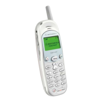
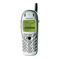
Topaz T2688/T200, T2988/T205 L3 Circuit Description
2
Motorola Proprietary Information
RECEIVE
1. Received GSM 900 frequency enters the unit at the Antenna ANT1
2. L501 / L502 / L503 provide matching
3. The signal then enters mechanical Auxiliary RF port U113. When a load (50? is
placed into the socket the RF will be diverted into or out of U113). This socket will
be used for phasing, testing purposes.
4. From U113 Pin 1 to RF Switch U501 Pin 9 (ANT), where through control voltages
the Rx path is isolated from the TX path. The following voltages control the RF
Switch: VC1 – VC4, which are all 0V or 3.6V Low or High respectively.
The controlling input signals are:
? BS (Band Select), this signal determines GSM (Logic 0) or DCS (Logic 1) –
2.8V (originates as BANDSW from Gemini Pin 65)
? PA_ON, this signal determines if the TX burst is on progress (for use with the
RF Switch only) – 2.8V (originates as TXPA from Gemini Pin 119)
? VBAT, is the battery voltage and supports both U502 which is the Logic control
for the RF switch and the inverter IC501 - 3.3V – 3.6V
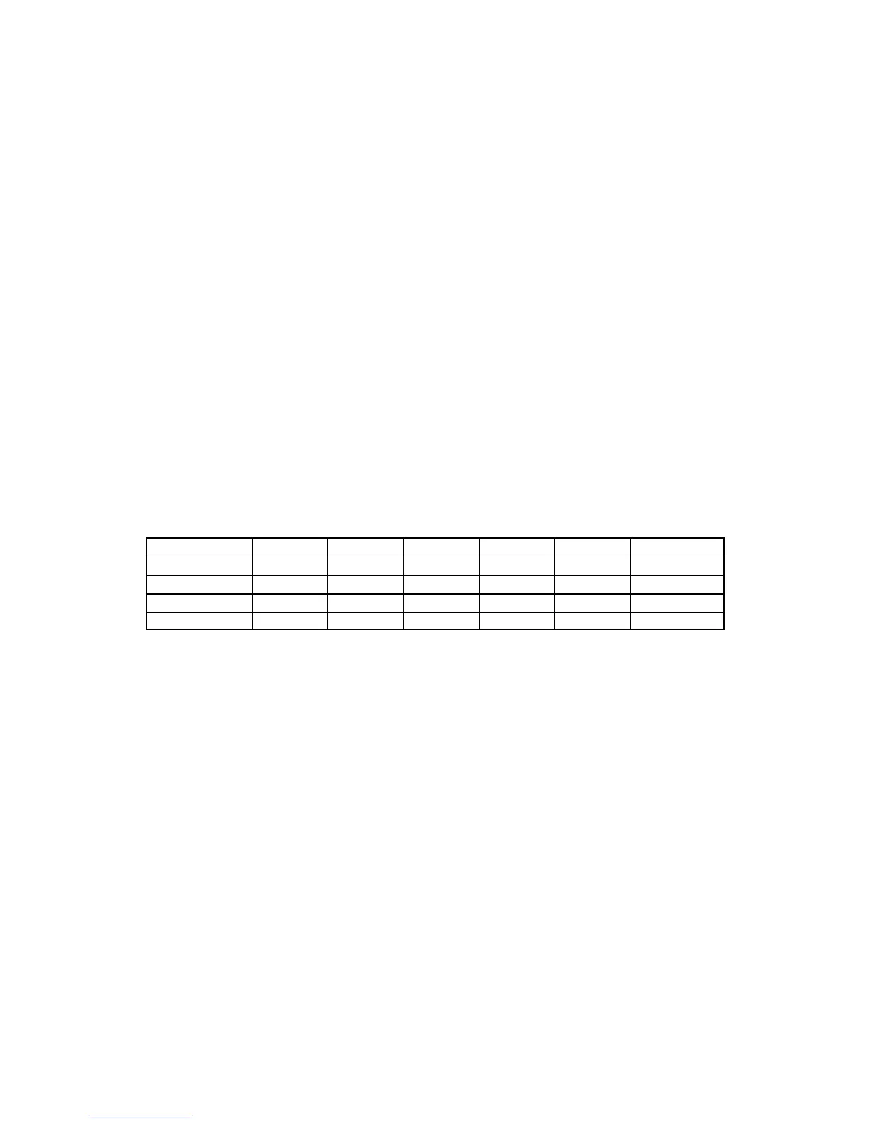
Below are the states of VC1 – VC4 and the relative states of BS and PA_ON for
each of the 4 scenarios.
VC1 VC2 VC3 VC4 BS PA_ON
GSM RX 0V 3.6V 3.6V 0V 0V 0V
GSM TX 3.6V 0V 3.6V 0V 0V 2.8V
DCS RX 0V 3.6V 3.6V 0V 2.8V 0V
DCS TX 0V 3.6V 0V 3.6V 2.8V 2.8V
5. The appropriate frequency is then fed out from U501 Pin 5 (GSM) GSM_RX or from
Pin 7 (DCS) DCS_RX.
6. The received frequency is then fed into a Dual Band select SAW (Standing Acoustic
Wave) filter U602 (Loss approximately 5dB). The GSM received frequency is then
applied to the base of Low Noise amplifier Q601, with input matching supplied by
C613 / L608 / C616 and the collector output matching elements supplied by C614 /
L607 / C606. The support voltage for Q601 and Q602 is from TX / RX IC U603 (see
Figure 1 for Block Schematic) Pin 3 (RFOUT) and is 2.1V when active. The bias
voltage that is approximately 1.4V will be used to switch the correct LNA on or off
dependant upon band selected, or mode of operation.
Q601 and Q602 are switched independently dependent upon the mode of the phone to
save power, this is provided by the 3 signals RXON1, RXON2 and TXON, U603
Pins 44, 45 & 46 respectively. (These signals originate as RXON, CALBRA and
TXEN from Gemini, Pins 70, 69 & 118 respectively) The signal BS, U603 Pin 35
selects the current operating band of the receiver. In addition, these signals allow the
phone to go into ‘Calibrate mode’ in between Receiver timeslots to allow the gain of
the PGA (Programmable Gain Amplifier) (this is internal to the IC) to be adjusted. It
 Loading...