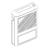
RPR 550IS Series
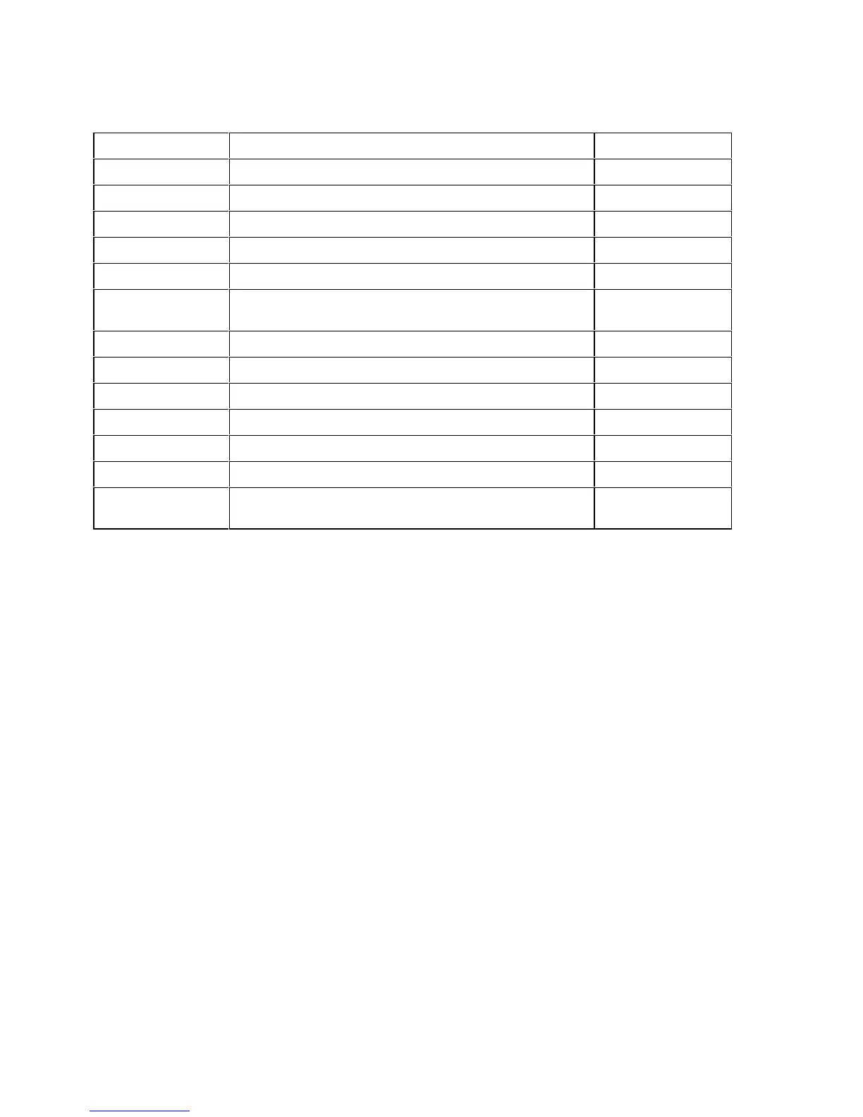
Table 4: RPR 550IS Main Board Decoder Circuit DC Voltage Levels
COMPONENT COLLECTOR BASE EMITTER REMARKS
TM1188 Issue 1Page 5 - 18
TR21a 0 (1) 0 (4) 0 (5) V
DD
2 regulation
TR21b 1.25 (2) 0 (4) 0 (3) "
TR22 0 0.87 1.21 V
DD
2 oscillator
TR23 1.49 0 0 Rack switch on
TR24 0 1.24 1.24 Beep enable amp
TR25a 1.49 (4) 0 (2) 0 (3) Charger pager
switch on
TR25b 1.49 (1) 0 (5) 0 (6) Charger pager reset
TR26 - 1.24 1.25 Vibrate enable
TR27 1.10 0.70 1.18 1V series regulator
TR28 0.70 1.14 0.80 1V regulation
TR29 1.08 1.59 1.07 Data filter gate
TR31a 0.02 (4) 0.50 (2) 0 (3) Data filter gate
TR31b 1.07 (1) 0.02/0.17 0 (6) Data filter switch
(5)
NOTES:
1. The voltages listed above were measured with a battery terminal voltage of
1.3V and SK2 pin 4 was connected to common. The radio board was not
connected, the speaker was connected and the pager was switched on.
2. Voltages may vary by approximately ±20mV between units.
3. The numbers in brackets refer to the pin number of the component.