1
2
3
4
6
7
8
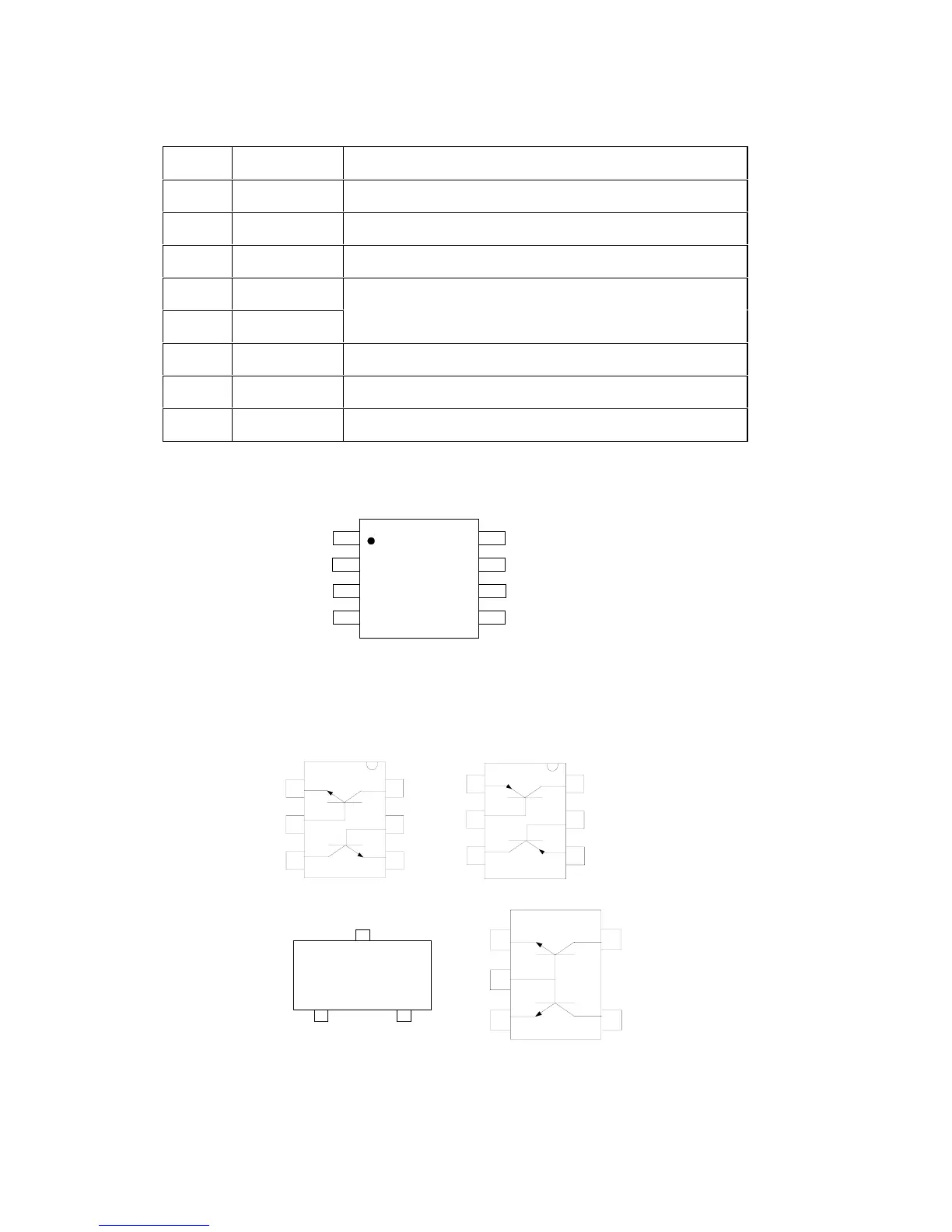
IC4
5
A0
VCC
TEST
SCL
SDA
A1
A2
VSS
PSG/10429/1
6
5
4
E
B
C
1
2
3
C
B
E
IMX1
4
5
6
E
B
C
1
2
3
C
B
E
IMT1
BE
TOP
2
1
3
BCX 17
2SD1757KS
DTA113ZU
C
1
2
3
4
5
E
B
E
FMW4
C
C
PSG/10428/1
RPR 550IS Series
Table 8: IC3, Microprocessor Pin Connections
PIN NAME DESCRIPTION
TM1188 Issue 1Page 5 - 26
Figure 9: IC4, EEPROM Pin Configuration
Figure 10: Semiconductor Lead Details
33 P13/TI0 To SCK (Sample Clock) on IC2
36 INT1/P11 To switch and timer interrupts on IC2
37 INT0/P10 To sync word detect on IC2
38 PGM
V
DD
I/P
39 V
DD
42 P21 Display RS O/P
43 P20 Display E O/P
44 P73 Battery Low I/P