Do you have a question about the NAD C510 and is the answer not in the manual?
Details on AES/EBU, SPDIF, HDMI, and USB audio inputs.
Details on HDMI Video Out, Analogue, and Trigger Out.
AC supply, power consumption, dimensions, and weight.
Circuit diagram for the main PCB's top layer.
Circuit diagram for the main PCB's audio section.
Circuit diagram for the main PCB's DDFA1 section.
Circuit diagram for the main PCB's HDMI section.
Circuit diagram for the main PCB's MCU section.
Circuit diagram for the main PCB's SPDIF section.
Circuit diagram for the main PCB's USB section.
Top and bottom layer views of the main circuit board.
Top and bottom layer views of the trigger board PCB.
Top and bottom layer views of the SMPS board PCB.
Top and bottom layer views of the FPP board PCB.
Top and bottom layer views of the VFD and Encode board PCB.
List of ICS, diodes, transistors, crystals, inductors, capacitors, etc. for the main PCB.
List of transistors, resistors, capacitors, connectors for the trigger board.
List of diodes, ICs, resistors, capacitors for the SMPS board.
List of ICS, diodes, transistors, inductors, capacitors, resistors for the FPP board.
List of resistors, capacitors, IR receiver, connectors for VFD/Encode boards.
| Sample rates | 32 - 192 kHz |
|---|---|
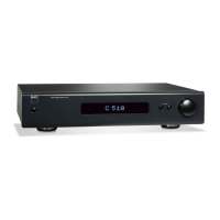
| Product color | Black |
| Frequency range | 20 - 96000 Hz |
| Signal-to-Noise Ratio (SNR) | -123 dB |
| Total Harmonic Distortion (THD) | 0.0005 % |
| DC output voltage | 2 V |
| Power supply input voltage | 100 - 240 V |
| Power consumption (standby) | 0.5 W |
| Power consumption (typical) | 16 W |
| Power supply input frequency | 50 - 60 Hz |
| Depth | 309 mm |
|---|---|
| Width | 435 mm |
| Height | 99 mm |
| Weight | 4700 g |
| Package weight | 5600 g |
| Quantity per pack | 1 pc(s) |