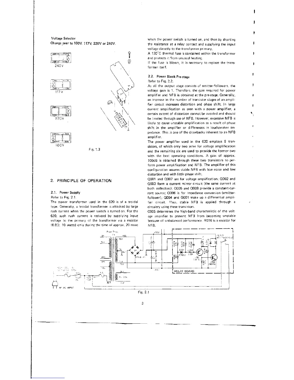
Voltage Selector
Change pverto 100V, 117V, 220V
or
240V.
240V
=
I
2 20V
=•
=
I
17 V
10
•
lo
—
I00V
240 V
240V—
81
j
220V—
117V
= I!7V
--H00V
1
2"
20 V—
J
l
—-\
7V
0
0
UV
220V
240V=^!
o
0
220 V—
IJ
ir-
II7V
!
'•—100V
1OOV
Fig.
1.3
2.
PRINCiPLE
OF
OPERATION
2.1.
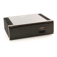
Power Supply
Refer
to
Fig. 2.1.
The power transformier used
in
the 620 is
of
a
troidai
type.
Generally,
a
troidai transformer
is
attacked
by
large
rush current when
the
power switch
is
turned on.
For the
620,
such rush current
is
reduced
by
suppiying input
voltage
to the
primary
of
the
transformer
via a
resistor
(6.8f2,
10
watts) only during
the
time
of
approx.
20
msec
when
the
power switch
is
turned on, and then
by
shorting
the resistance
at a
relay contact
and
suppiying
the
input
voltage directly
to
the
transformer primary.
A 130"C thermal fuse
is
contained within
the
transformer
and protects
it
from unusual heating.
lf
the
fuse
is
blown,
it
is
necessary
to
replace
the
trans-
former itself.
2.2. Power Block Pre-stage
Refer
to
Fig.
2.2.
As
all the
Output stage consists
of
emitter-followers,
the
voltage gain
is
1.
Therefore,
the
gain required
for
power
amplifier
and NFB
is
obtained
at
the pre-stage. Generally,
an increase
in
the
number
of
transistor stages
of
an
ampli-
fier circuit increases distortion
and
phase shift.
In
large
current amplification
as
seen with
a
power amplifier,
a
certain extent
of
distortion cannot be avoided and should
be limited through use
of
NFB. However, excessive
NFB
is
likely
to
cause unstable amplification
as a
result
of
phase
shift
in
the
amplifier
or
differences
in
Soudspeaker
im-
pedance. This
is
one
of
the drawbacks inherent
to an NFB
amplifier.
The power amplifier used
in
the 620
employs
8
tran-
sistors,
of
which only
two
serve
for
voltage amplification
and
the
remaining
six are
used
to
provide
the
former
two
with
the
best operating conditions.
A
gain
of
approx.
100dB
is
obtained through these
two
transistors
to
per-
form power amplification
and
NFB.
The
amplifier
of
this
configuration assures stable
NFB
with
!ow
noise
and
Iow
distortion and with little phase shift.
Q001
and
Q007
are
for
voltage amplification; Q002
and
Q003 form
a
current mirror circuit
(the
same current
at
both collectors); Q005
and
Q008 provide
a
constant-cur-
rent source; Q006
is for
impedance conversion (emitter-
follower); Q004
and Q001
make
up
a
differential ampli-
fier circuit. Thus, stable
NFB
is
applied through
a
circuitry using these transistors.
C005 determines
the
high-band characteristic
of
the
volt-
age amplifier
to
prevent
NFB
from becoming unstable
because
of
unbalanced Performance. R016
is
a resistor
for
NFB.
2.1
 Loading...