B-28 | ni.com
Appendix B Timing Diagrams
Digital I/O Timing Diagrams
This section describes the timing delays and requirements of digital waveform acquisitions and
digital waveform generations.
Digital Waveform Acquisition Timing
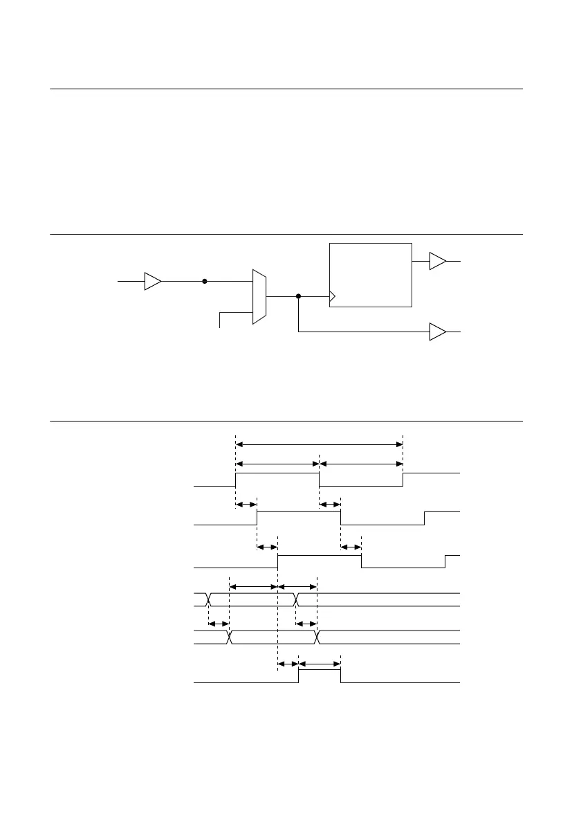
To describe digital waveform acquisition timing delays and requirements, refer to the circuitry
shown in Figure B-37. In the figure, P0, PFI, RTSI, and PXI_STAR represent signals at
connector pins of the M Series device. The other named signals represent internal signals.
Figure B-37. Digital Waveform Acquisition Timing Circuitry
Figure B-38 and Tables B-22 and B-23 describe the digital waveform acquisition timing delays
and requirements. Your inputs must meet the requirements to ensure proper behavior.
Figure B-38. Digital Waveform Acquisition Timing Delays
DO Waveform
Generation FIFO
PFI (Output)
P0
DO Sample
Clock
Other Internal
Signals
PFI_i, RTSI_i,
or PXI_STAR_i
PFI, RTSI,
or PXI_STA R
PFI, RTSI,
or PXI_STA R
PFI_i, RTSI_i,
or PXI_STAR_i
t
1
t
2
t
3
t
3
t
2
t
4
t
4
t
7
t
8
t
9
t
5
t
6
t
7
PFI (Output)
DI Sample Clock
P0
P0_i
 Loading...