B-30 | ni.com
Appendix B Timing Diagrams
Digital Waveform Generation Timing
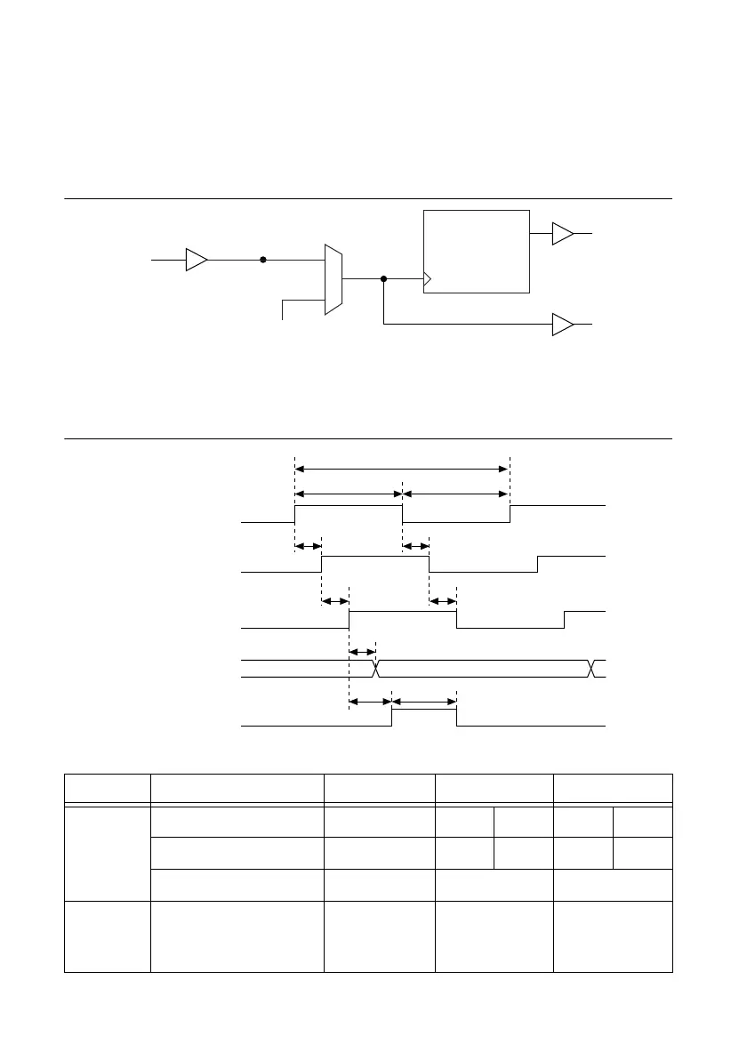
To describe digital waveform generation timing delays and requirements, we model the circuitry
as shown in Figure B-39. In the figure, P0, PFI, RTSI, and PXI_STAR represent signals at
connector pins of the M Series device. The other named signals represent internal signals.
Figure B-39. Digital Waveform Generation Timing Circuitry
Figure B-40 and Tables B-24 and B-25 describe the digital waveform generation timing delays
and requirements. Your inputs must meet the requirements to ensure proper behavior.
Figure B-40. Digital Waveform Acquisition Timing Delays
Table B-24. DO Timing Delays
Time From To Min (ns) Max (ns)
t
12
*
PFI PFI_i 5.2 6.2 18.2 22.0
RTSI RTSI_i 2.0 2.5 5.0 6.0
PXI_STAR PXI_STAR_i 1.5 3.5
t
13
PFI_i, RTSI_i,
PXI_STAR_i, or other
internal signal
DO Sample
Clock
3.5 9.5
DO Waveform
Generation FIFO
PFI (Output)
P0
DO Sample
Clock
Other Internal
Signals
PFI_i, RTSI_i,
or PXI_STAR_i
PFI, RTSI,
or PXI_STA R
PFI, RTSI,
or PXI_STA R
PFI_i, RTSI_i,
or PXI_STAR_i
t
10
t
11
t
12
t
12
t
11
t
13
t
13
t
15
t
16
t
14
DO Sample Clock
P0
PFI (Output)
 Loading...