B-32 | ni.com
Appendix B Timing Diagrams
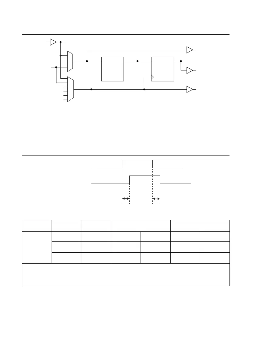
Figure B-41. Counter/Timer Circuitry
Pin to Internal Signal Delays
Input timing is the timing specification for importing a signal to an internal bus on the M Series
device. Table B-26 shows the input timing for the counters on all input terminals. Signals refer
to the signal at the I/O connector of the device, and signals appended with _i refer to the signal
internal to the device after the input buffer.
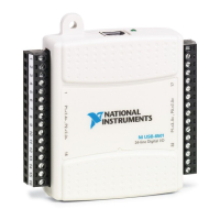
Figure B-42. Pin to Internal Signal Delays Timing Diagram
Table B-26. Pin to Internal Signal Delays Timing
Time From To Min (ns) Max (ns)
t
1
*
PFI PFI_i 5.2 6.2 18.2 22.0
RTSI RTSI_i 2.0 2.5 5.0 6.0
STAR STAR_i 0.9 — — 2.5
*
The delay ranges given for PFI and RTSI represent the fastest and slowest terminal routing within the
trigger group for a given condition (maximum or minimum timing). This difference can be useful when
two external signals will be used together and the relative timing between the signals is important.
32-Bit
Counter
Gate
Logic
PFI, RTSI,
or PXI_STA R
(Counter n Source)
PFI, RTSI,
or PXI_STA R
(Counter n Gate)
PFI, RTSI,
or PXI_STA R
(Counter n
Internal Output)
Count_Enable
Other Internal
Signals
PFI_i, RTSI_i,
or PXI_STAR_i
Selected_Gate
Selected_Source
Out_o
PFI, RTSI,
or PXI_STA R
80 MHz Timebase
20 MHz Timebase
100 kHz Timebase
PXICLK10
t
1
t
1
PFI, RTSI,
or PXI_STA R
PFI_i, RTSI_i,
or PXI_STAR_i
 Loading...