© National Instruments | B-27
M Series User Manual
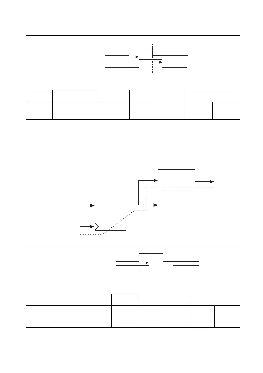
Figure B-34. Pause Trigger Output Routing Delay Timing Diagram
• Sample Clock—The rising edge of the Sample Clock is output synchronous to the Sample
Clock Timebase. It can be calculated by adding the Sample Clock Timebase insertion to the
delay in Table B-21. The exported Sample Clock signal is active low, each falling edge
representing a conversion.
Figure B-35. Sample Clock Path
Figure B-36. Sample Clock Delay Timing Diagram
Table B-20. Pause Trigger Output Routing Delay Timing
Time From To Min (ns) Max (ns)
t
13
Selected Pause
Trigger
RTSI 6.7 7.1 16.3 17.0
Table B-21. Sample Clock Delay Timing
Time From To Min (ns) Max (ns)
t
14
AO Sample Clock PFI 9.7 10.7 31.1 34.3
AO Sample Clock RTSI 8.8 9.1 21.3 21.7
Selected Pause Trigger
RTSI Terminal
t
13
t
13
Internal Logic
Sample Clock Timebase
DQ
To Internal Logic
Routing Logic
RTSI, PFI
Sample Clock Timebase
RTSI/PFI Terminal
t
14
 Loading...