© National Instruments Corporation 4-1 PCI/PXI-6703/6704 User Manual
4
Hardware Overview
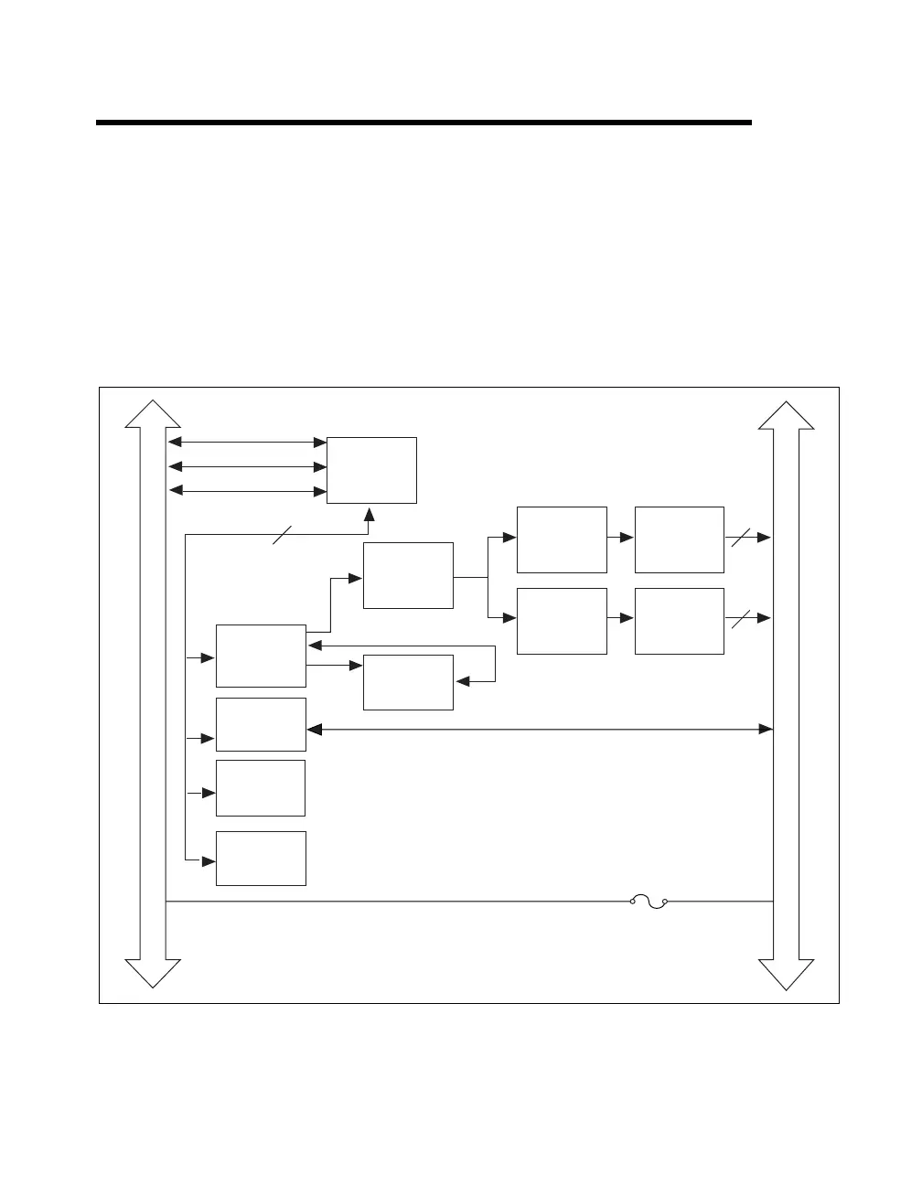
This chapter contains a functional overview of the 6703/6704 devices and
explains the operation of each functional unit making up the devices.
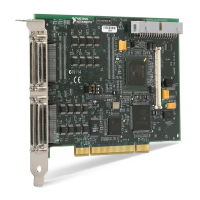
The block diagram in Figure 4-1 illustrates the key functional components
of the 6703/6704 devices.
Figure 4-1.
PCI/PXI-6703/6704 Block Diagram
PCI/PXI Bus
I/O Connector
Control
Address
Data
Bus
Interface
Logic
nvRAM/
DAC
Control
Digital
I/O
16-Bit
DAC
nvSRAM
Main
Voltage
Circuit
Main
Current
Circuit*
Voltage
Output
Circuit X 16
Current
Output
Circuit X 16*
RAM
Addr/Ctrl
RAM Data
DAC
Out
Control
Lines
DIO Lines <7..0>
16
16
0.75 A
Self-Resetting Circuit Breaker
+5 V
Serial
Number
EEPROM
Temperature
Sensor
*No current circuits present on PCI/PXI-6703
 Loading...