NI sbRIO-961x/9612XT/963x/9632XT/964x/9642XT 24 ni.com
Integrated 3.3 V Digital I/O
The four 50-pin IDC headers, P2–P5, provide connections for
110 low-voltage DIO channels, 82 D GND, and eight +5 V voltage outputs.
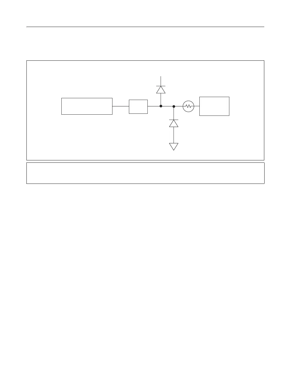
Figure 16 represents a single DIO channel.
Figure 16. Circuitry of One 3.3 V DIO Channel
I/O Protection
The 33 Ω current-limiting posistor, R1, and the protection diodes, D1 and
D2, protect each DIO channel against externally applied voltages and ESD
events. The combination of R1 and D1 protects against overvoltage,
and the combination of R1 and D2 protects against undervoltage. The
resistance of R1 increases rapidly with temperature. During overvoltage
conditions, high current flows through R1 and into the protection diodes.
High current causes internal heating in the posistor, which increases the
resistance and limits the current. Refer to the Specifications section for
current-limiting and resistance values.
Drive Strength
The NI sbRIO devices are tested with all 110 DIO channels driving 3 mA
DC loads, for a total of 330 mA sourcing from the FPGA. The FPGA uses
minimum 8 mA drivers, but the devices are not characterized for loads
higher than 3 mA.
U1: 5 V to 3.3 V Level Shifter, SN74CBTD3384CDGV from Texas Instruments
D1 and D2: ESD-Rated Protection Diodes, NUP4302MR6T1G from ON Semiconductor
R1: Current-Limiting Posistor, PRG18BB330MS1RB from Murata
User
Connection
Xilinx Spartan-3 FPGA
U1
+5 V
D2
D1
R1
 Loading...