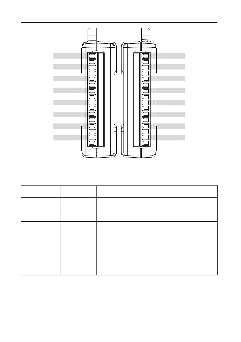
Figure 5. NI USB-6501 Device Pinout
P0.0
P0.1
P0.2
P0.3
P0.4
P0.5
P0.6
P0.7
GND
GND
P1.0
P1.1
P1.2
P1.3
+5V
GND
GND
+5V
P1.7
P1.6
P1.5
P1.4
GND
GND
P2.7/PFI 0
P2.6
P2.5
P2.4
P2.3
P2.2
P2.1
P2.0
GND +5V P1.3P1.2P1.1P1.0GND GNDP0.7P0.6 P0.5 P0.4P0.3P0.2 P0.1P0.0
GND +5V P1.7P1.6P1.5P1.4GND GNDP2.7P2.6 P2.5 P2.4P2.3P2.2 P2.1P2.0
The following table describes the signals available on the I/O connectors.
Table 2. Signal Descriptions
Signal Name Direction Description
P0.<0..7>,
P1.<0..7>,
P2.<0..6>
Input or Output Digital I/O Signals: You can individually configure
each signal as an input or output.
P2.7/PFI 0 Input or Output This pin is configurable as either a digital line or an
event counter.
Digital I/O Signal: As a digital line, this signal can be
used as an input or output.
CTR: As a counter, this signal can be used as an event
counter input source.
NI USB-6501 User Guide | © National Instruments | 7
 Loading...