NI USRP-2953R
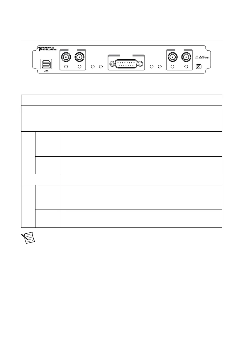
Figure 24. NI USRP-2953R Front Panel
LINK
TX OUTPUT MAX +20 dBm, RX INPUT MAX -15 dBm, ALL RF PORTS 50 Ω
TX1 RX1 RX2GPSPPSREF
TX1 RX1 RX2
RF 0 RF 1
JTAG
AUX I/O
3.3 VDC MAX
NI USRP-2953R
1
.2 GHz - 6 GHz
Designed by Ettus ResearchDesigned by Ettus Research
PWR
Table 31. NI USRP-2953R Module Front Panel Connectors
Connector Use
JTAG A USB port that connects the host computer to the device FPGA for
development and debugging. LabVIEW FPGA does not currently support
configuring or programming the device FPGA using the JTAG connector.
RF 0 TX1 RX1 Input and output terminal for the RF signal. TX1 RX1 is an SMA (f)
connector with an impedance of 50
Ω and is a single-ended input or output
channel.
RX2 Input terminal for the RF signal. RX2 is an SMA (f) connector with an
impedance of 50 Ω and is a single-ended input channel.
AUX I/O General-purpose I/O (GPIO) port. AUX I/O is controlled by the FPGA.
RF 1 TX1 RX1 Input and output terminal for the RF signal. TX1 RX1 is an SMA (f)
connector with an impedance of 50 Ω and is a single-ended input or output
channel.
RX2 Input terminal for the RF signal. RX2 is an SMA (f) connector with an
impedance of 50 Ω and is a single-ended input channel.
Note The LED indications described in the following table occur only when you
use the NI-USRP
API with the default FPGA image. When you use LabVIEW
FPGA, you customize the LED indications.
NI USRP-29xx Getting Started Guide
| © National Instruments | 49