NI Digital System Development Board User Manual | © National Instruments | 27
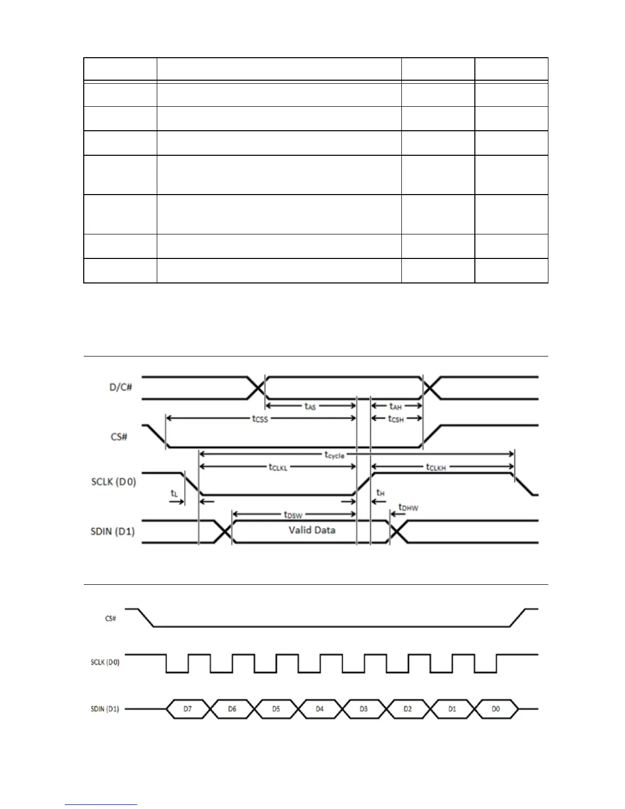
The serial interface is synchronous to SCLK and must conform to the timing specifications
below. In most cases, a 10 MHz SCLK and data sent on the falling edge should work.
Figure 8. Serial Interface Timing Diagram
Figure 9. OLED Serial Interface Bit Ordering
Table 11. OLED Signal Description
Signal Description Polarity FPGA Pin
RES# Reset Active-low E16
CS# Chip select (always active) Active-low N/A
D/C# Data (high)/Command (low) Both H15
SCLK Serial Clock Active-hig
h
J15
SDIN Serial Data Active-hig
h
J17
VBAT# Power enable for internal power supply Active-low L17
VDD# Power enable for digital power Active-low J16
 Loading...