NI Digital System Development Board User Manual | © National Instruments | 59
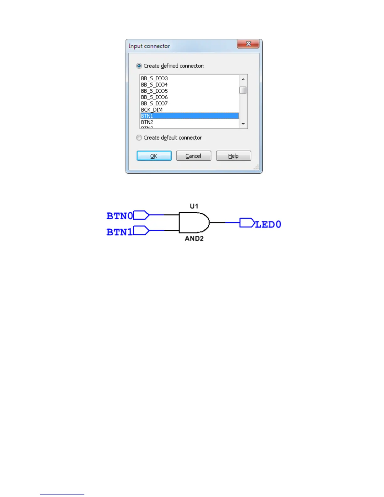
4. Select the push button BTN1 and click OK.
5. Wire the AND gate to the connectors.
Export the PLD Design to the FPGA
There are three options for exporting the digital logic from the PLD schematic:
• Programming the connected PLD—Allows students to deploy the design directly to
the FPGA.
• Generate and save a programming file—Students can generate a bitfile that can be used
to program hardware later.
• Generate and save the VHDL—This option exports the VHDL netlist, allowing students
to view the VHDL code. You can import the VHDL code in the Xilinx environment and
program the FPGA
 Loading...