7-11
3.2 Inverter
Input interface section:
1. 12V DC input, , provided by power section;
2. ON/OFF enable signal, , provided by GMZAN3SL from the main board with value of 0Vor 3V. When
OFF=0V, the inverter doesn’t work, while OFF=3V, it works under normal situation.
3. DIM signal for luminance modulation, offered by GMZAN3SL in the main board with its range of 0~5V.
The Inverter offers different currents to the loads because of the different feedback of voltage to the
feedback-terminal of PWM. The smaller the value of DIM, the smaller the current output of Inverter, the
darker the brightness.
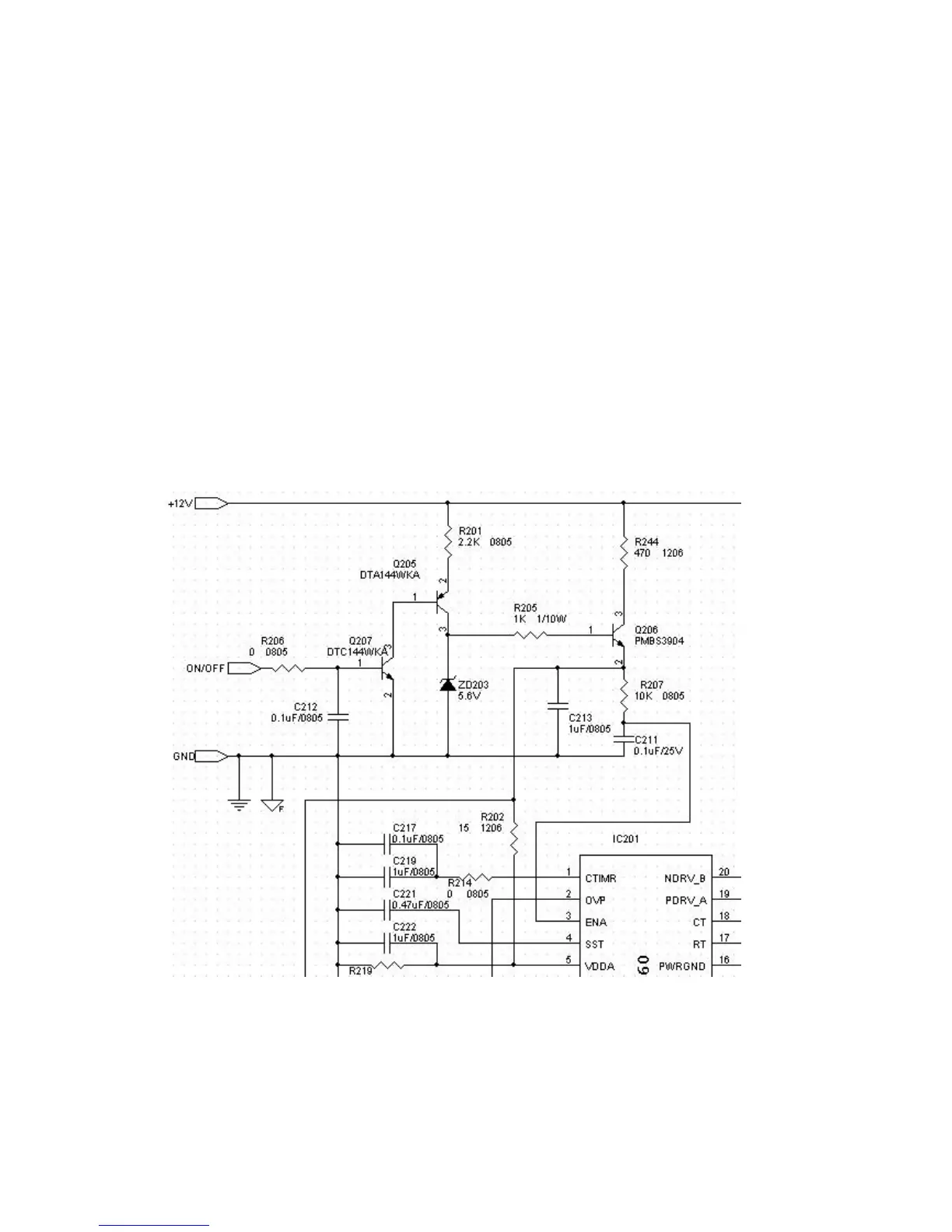
Voltage start-up circuit: It consists of a PNP, and two NPN transistors with two working stages. The first
stage: When the ON/OFF enable voltage is 0V, Q207, Q205 and Q206 are closed. So the DC voltage at the
emitter of Q206 can’t be applied to PIN 3 and PIN 5 of IC201. The inverter will not work because there are no
pulse output at PIN 11, PIN 12, PIN 19 and PIN 20. . The second stage: When the ON/OFF enable voltage is
high, Q207, Q205 and Q206 get through. Then 12V voltage is applied to PIN 3 and PIN 5 of IC201 resulting in
the operation of the IC. IC201 produces a pulse output to the control switch transistor, and the Inverter work
applying high voltage to the backlight.