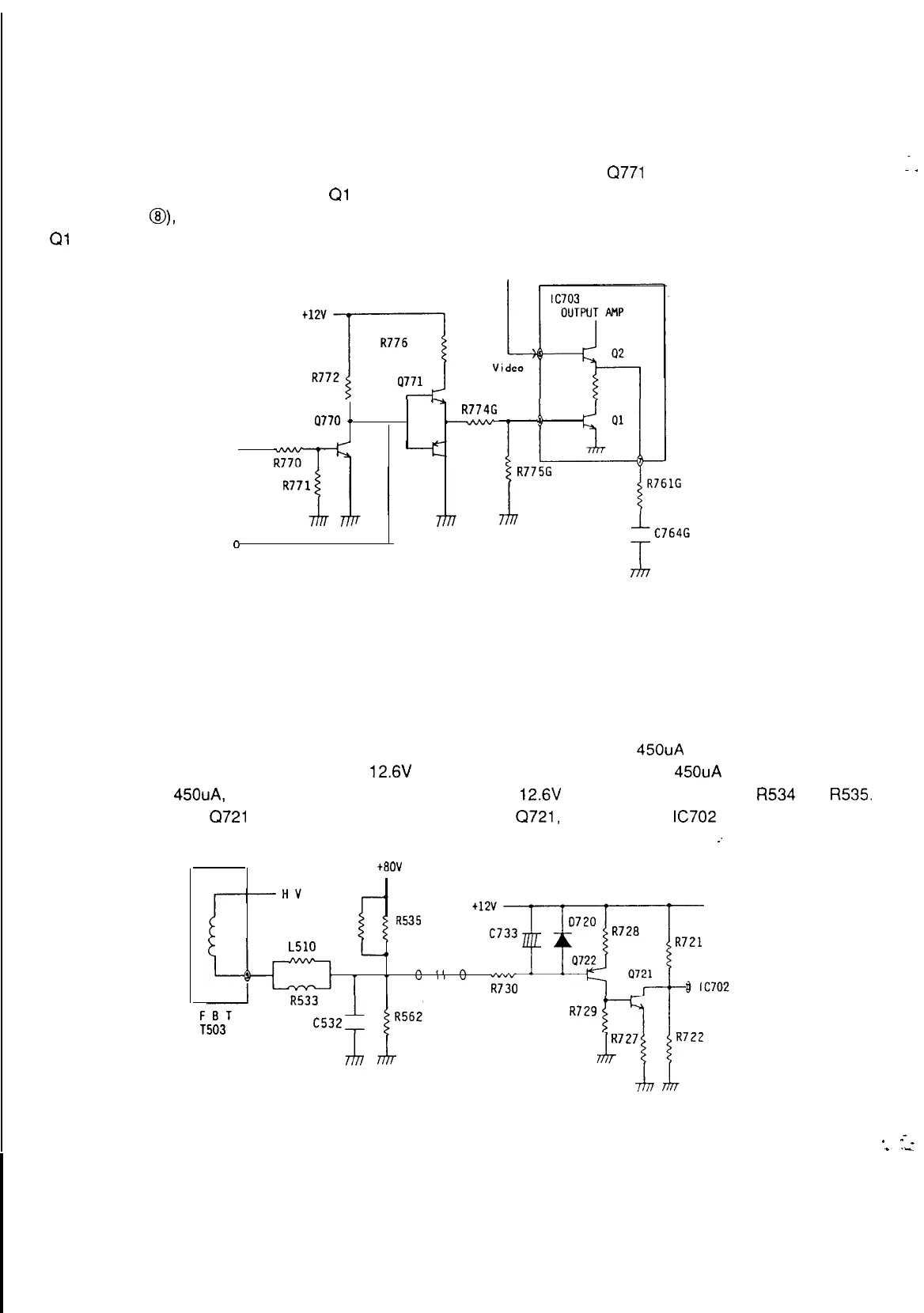
3-3. Video Blanking Circuit and Video Mute Circuit
The H blanking pulse is applied to the push pull circuit which is composed of
Cl771
and Q772. During the blanking
:
.
period this pulse turn on the transistor
Ql
and the video amplifier at cut-off. The video mute signal is generated at
the CPU (pin
@I),
when input signal is changed. Q770 is turned on by the video mute signal from the CPU. Then
Ql
is turned off and the video amplifier is cut-off during the time that the video mute signal is generated.
‘y
R774G
0770
0
w
A8
VIDEO MUTE
0
0772
J4
7777
0
T
BLANKING PULSE
77i7
(Fig 3-3-l) Video Blanking and Mute Circuit
3-4. ABL Circuit
The maximum average current flowing through the CRT is’ controlled to under 450uA by limiting the video Vp-p
swing. The voltage of CN-J3 is clamped at
12.6V
by 0720 when the anode current is 450uA or less. If the anode
current exceeds 450uA, the voltage of CN-J3 drops to less than
12.6V
due to the voltage drop of
FE34
and
R535.
This drives Q722 and
Q721
to decrease the collector potential of
Q721,
and the gain of
IC702
is decrease.
:
taov
0
R534
CN-J3
FBT
T503
c532
(Fig 3-4-l) ABL Circuit
54
.
*-_
.
._