JR1 Signal XP3 Contact JR1 Pin Description
V1- G 4 Negative voltage/Return for signal 1
V2+ F 7 Positive voltage for signal 2
V2- E 3 Negative voltage/Return for signal 2
V3+ D 6 Positive voltage for signal 3
V3- C 2 Negative voltage/Return for signal 3
V4+ B 5 Positive voltage for signal 4
V4- A 1 Negative voltage/Return for signal 4
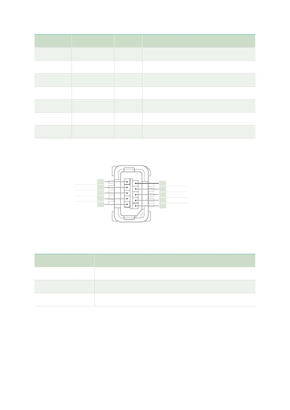
Figure 4 : JR2 — JR9 Pinout
IO x.H
IO x.G
AUX/GND (J)
IO x.F
IO x.E
IO x.A
IO x.B
REF/GND (I)
IO x.C
IO x.D
10
9
8
7
6
1
2
3
4
5
Table 2 : JR2 — JR9 Connector Signal Descrip
tions
Signal Description
IO x.
y Element y
in Bank x
REF/GND (I) Reference connection, signal ground
AUX/GND (J) Auxiliary connection, shorted to REF/GND
6 ni.com
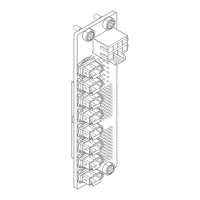
RTI-12309 Getting Started
 Loading...