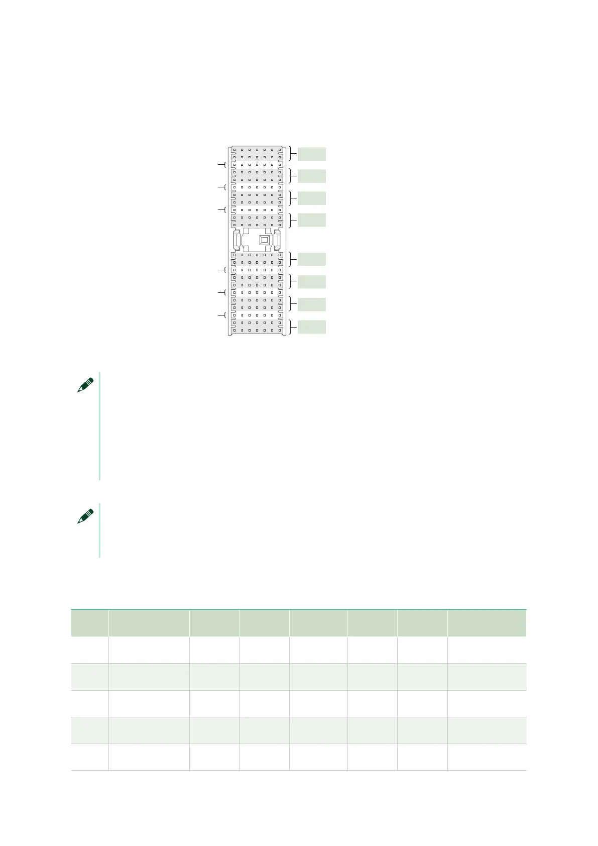
Figure 5 : XP2 Connector Or
ganization
XP2
d e fc
b
az
GND A
1
11
15
25
GND A
GND A
GND B
GND B
GND B
Bank 1
Bank 2
Bank 3
Bank 4
IO 7.x
IO 8.x
Bank 5
Bank 6
Bank 7
Bank 8
IO 2.x
IO 3.x
IO 4.x
IO 1.x
IO 6.x
IO 5.x
NOTE
Column z pins are tied to GND A or B on the R
TI-12309, and are designed to contact
an optional lower shield on the SLSC module connector, if the shield is present.
Column f pins are all no-connects (NC) on the RTI-12309, and are designed to
contact the same upper shield on the SLSC module connector. The SLSC module
designer configures these pins as GND A or GND B.
NOTE
JR2-5 (Banks 1-4) ar
e r
ef
erenced/routed to GND A on the XP2 connector, and JR6-9
(Banks 5-8) are referenced/routed to GND B on the XP2 connector.
Table 4 : XP2 Input/Output Pin A
ssignments
Row z a b c d e f
1 GND A (NC) IO 1.A IO 1.B RSVD0 IO 1.C IO 1.D GND X (NC)
2 GND A (NC) IO 1.E IO 1.F RSVD1 IO 1.G IO 1.H GND X (NC)
3 GND A (NC) GND A GND A GND A GND A GND A GND X (NC)
4 GND A (NC) IO 2.A IO 2.B RSVD2 IO 2.C IO 2.D GND X (NC)
5 GND A (NC) IO 2.E IO 2.F RSVD3 IO 2.G IO 2.H GND X (NC)
8 ni.com
RTI-12309 Getting Started
 Loading...