CIRCUIT DESCRIPTION
NI KKO'
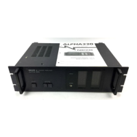
s ALPHA 220
, adopting latest
devices such as
Hi-
tT power transistors
, is of a design introducing a variable
bias circuit (non-switching circuit), a DC
servo circuit and
other most advanced techniques.
For details
, refer to
page 2 "
BLOCK DIAGRAM"
and page 8 "
SCHEMATIC DIAGRAM"
The following are
explanations of the main
circuits
and devices.
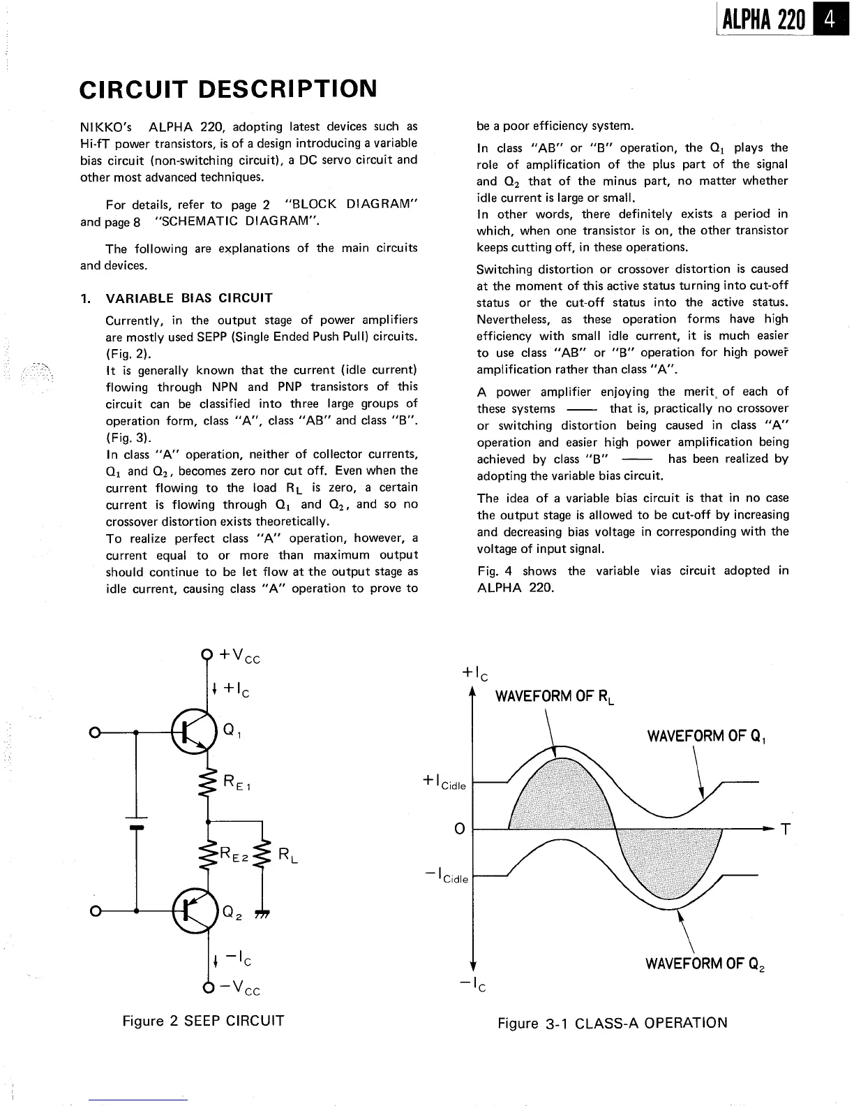
VARIABLE BIAS CIRCUIT
Currently, in the output
stage of power
amplifiers
are mostly used SEPP (Single Ended Push Pull) circuits.
(Fig. 2).
It is generally
known that the current (idle
current)
flowing through NPN and PNP
transistors of this
circuit can be
classified into three large
groups of
operation form,
class " , class "AB" and class "
(Fig. 3).
In class "A" operation
, neither of collector currents
01 and O2, becomes zero
nor cut off. Even when the
current flowing to the load
RL is zero
, a certain
current is flowing through 01
and O2, and so no
crossover distortion exists theoretically.
To
real ize
perfect class
" A" operation
, however
, a
current equal to or
more than maximum
output
should continue to be let
flow at the output stage as
idle current, causing class
" A" operation to
prove to
+Vee
RE2
Figure 2 SEEP CIRCUIT
eidle
eidle
I ALPHA 220
be a poor efficiency system.
In class "AB" or "
B" operation
, the 01
plays the
role of amplification of the plus part of the
signal
and O2 that of the minus part
, no matter whether
idle current is large or small.
I n other words
, there definitely exists a period in
which, when one transistor is on
, the other transistor
keeps cutting off
, in these operations.
Switching distortion or
crossover distortion is caused
at the moment of this active
status turning into cut-off
status or the cut-off
status into the
active status.
Nevertheless
, as
these operation forms have
high
efficiency with small idle current
, it is much easier
to use
class "
AB" or "B" operation for high power
amplification rather than class "
power amplifier enjoying the merit
, of each of
these systems that is
, practically no crossover
or switching distortion being caused in
class "
operation and
easier high power amplification
being
achieved by
class "
B"
has been realized by
adopting the variable bias circuit.
The idea of a
variable bias circuit is that in no
case
the output stage is allowed to be cut-off by
increasing
and decreasing bias voltage in corresponding with the
voltage of input signal.
Fig. 4 shows the
variable vias circuit adopted in
ALPHA 220.
WAVEFORM OF R
WAVEFORM OF QI
WAVEFORM OF Q2
Figure 3-
1 CLASS-
A OPERATION