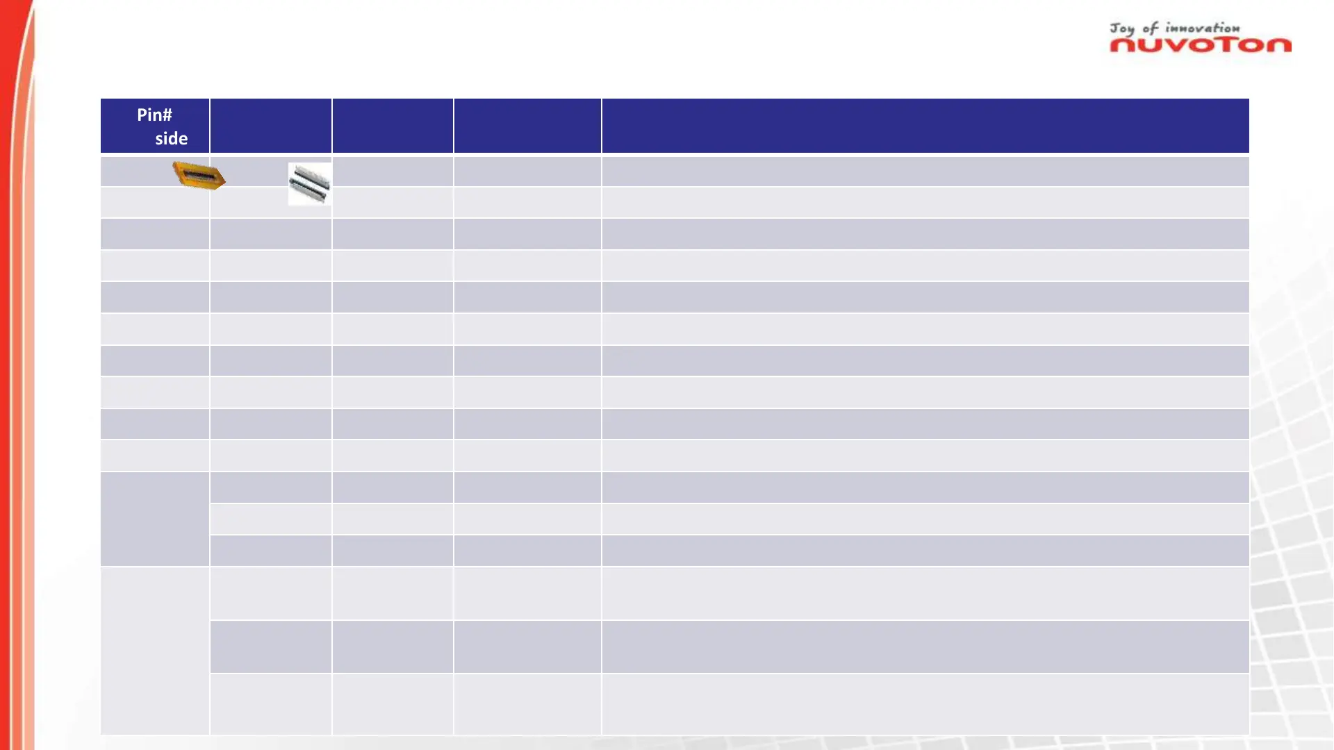
9
Pin#
SoC side
Pin#
ToF side
Pin Name Function Remark
21 1 CLKP MIPI Clock
MIPI clock input of positive
MIPI clock input of negative
MIPI data input of positive for lane#0
MIPI data input of negative for lane#0
MIPI data input of positive for lane#1
MIPI data input of negative for lane #1
Should be connected to I2C clock output terminal on
Should be connected to I2C data terminal on
SoC
5 9 RSTB_SYNC RESET / SYNC
27 10 AFE_GPO5 Field Index
Should be connected to EX
-IRQ input terminal for both edge on SoC
GND
6, 9, 12, 15,
19, 22, 24,
11 GND GND
– and GND connection pin for SoM board
12 GND GND
– and GND connection pin for SoM board
13 GND GND
– and GND connection pin for SoM board
VCC
3, 28, 30
+
16*
*need 5V
input
14 VCC Power supply
input
Connect to DC jack or QCOM board Power
Supply (5V・max 3.0A)
15 VCC Power supply
input
Connect to DC jack or QCOM board Power
Supply (5V・max 3.0A)
16 VCC Power supply
input
Connect to DC jack or QCOM board Power
Supply (5V・max 3.0A)
Pin assignment of Adapter Board for KHKT001-EVM side and SoC side
 Loading...