7. Connection Diagram
Oki Data CONFIDENTIAL
44983601TH Rev.1
7-7 /
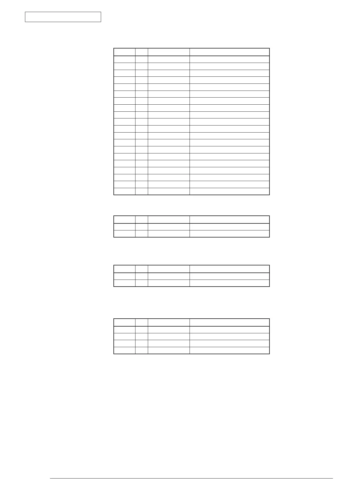
• HEAD0ConnectorPinAllocation
(ConnectiontheLEDHEADAssy)
• THERMConnectorPinAllocation
(Connection to the thermistor sensor)
• FACEUPConnectorPinAllocation
(ConnectiontotheFaceUp/DownSwitch)
• EXITMConnectorPinAllocation
(Connection to the Exit Motor)
PinNo. I/O Signal Function
1 C VSS Logic Ground
2 O CLKP Clock
3 O CLKN Clock
4 C VSS Logic Ground
5 O LOAD Load
6 O HSYNCN Synchronizingsignal
7 O D3 Data 3
8 O D2 Data 2
9 O D1 Data 1
10 O D0 Data 0
11 O STBN Strobe
12 O SCK SerialClock
13 I SO SerialData
14 O 3.3V LogicPower
15 C GND LED Ground
16 O VDD LEDDrivePower
17 C GND LED Ground
18 O VDD LEDDrivePower
19 C GND LED Ground
20 O VDD LEDDrivePower
PinNo. I/O Signal Function
1 +3.3V ThermistorPowerVoltage
2 THERM FusingTemperatureDetection
PinNo. I/O Signal Function
1 FACEUP-N Faceup/downchange
2 0V AnalogGround
PinNo. I/O Signal Function
1 O HOP1 MotorDrivePower
2 O HOP2 MotorDrivePower
3 O HOP3 MotorDrivePower
4 O HOP4 MotorDrivePower