FM Transmitter
Sistemas Electrónicos S.A EM 100 DIG
Technical Manual - v1.2 - November 2005 45
Elements numbered in Figure 3-3 can be described as follows:
1 - Input splitter transformer and coupling circuit.
2 - Bias adjustment potentiometer.
3 - Bias regulator circuit.
4 - MOSFET push-pull arranged, twin-transistor capsule.
5 - Output combiner transformer and matching circuit.
Following this amplifier stage, module includes a low-pass filter in order to attenuate or suppress all
harmonics and IM products beyond Band II limits, as shown in Figure 3-4:
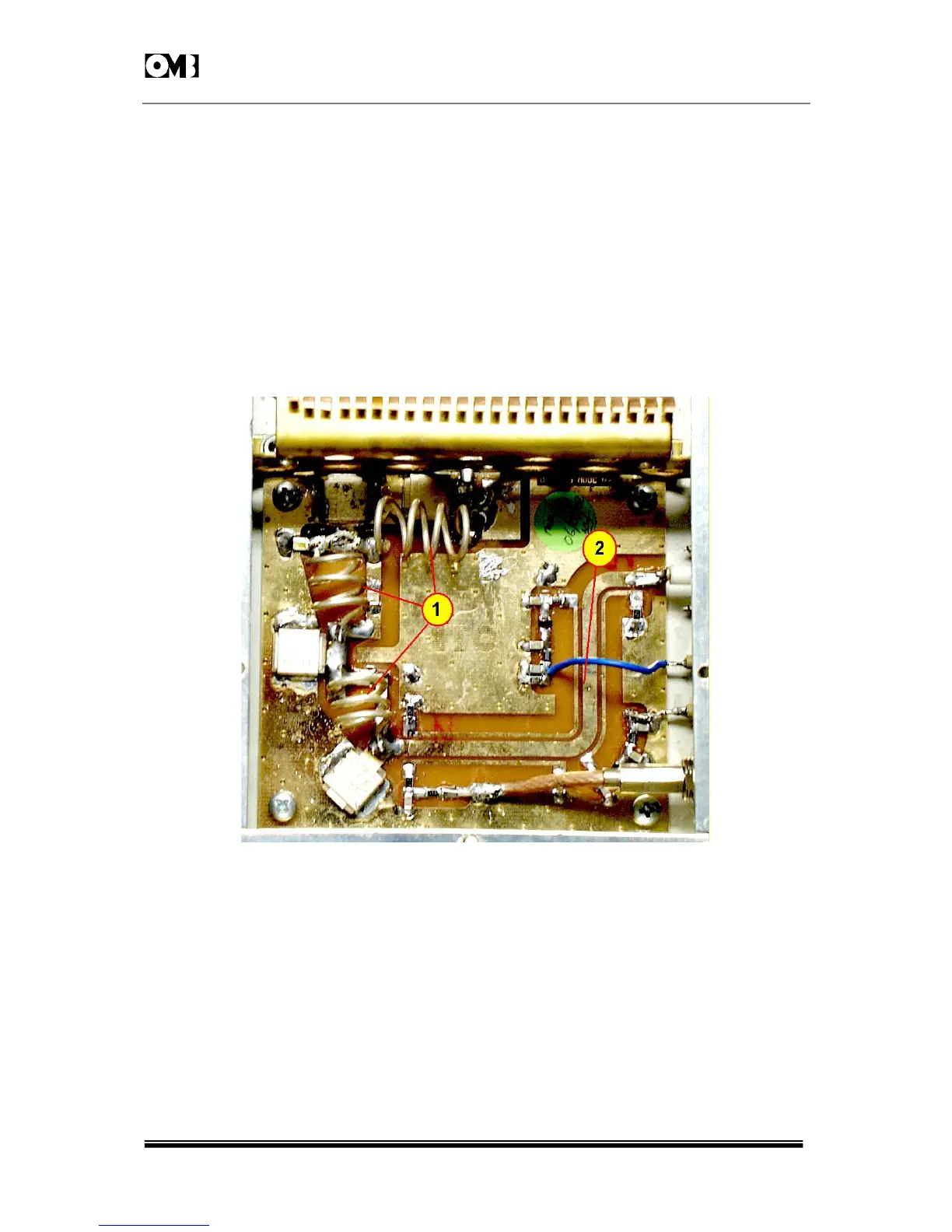
Fig. 3-4: DETAILED VIEW OF LOW-PASS FILTER and DIRECTIONAL COUPLER SECTION.
The three-sections low-pass filter (1) attenuates the harmonics to a value that is generally below
-70dBc, following the output transistor drain circuit. Also, included in the RF output path, a directional
coupler (2) generates a dc signal, which is proportional to the forward and reflected RF power, and
a RF non-demodulated sample (RF MONITOR) to be externally used by a frequency counter or a
modulation monitor, for measurements purposes.
The transistor gate is biased by a Zener network and a potentiometer which adjusts the idle current of
the transistor. Varying the control voltage towards a negative supply progressively disables the
amplifier transistor, so effectively acting as an AGC input. In fact the power management circuit, in a
closed loop driven by the output sensor circuitry, varies this voltage. This will accordingly vary the
output power to obtain the pre-set value and cope with alarm and start-up conditions.