MC14541B
www.onsemi.com
2
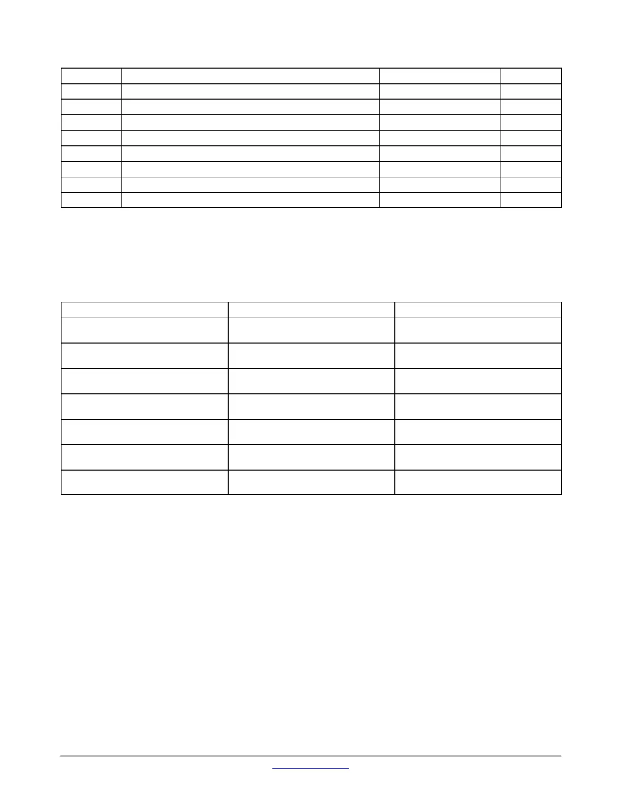
MAXIMUM RATINGS (Voltages Referenced to V
SS
)
Symbol
Parameter Value Unit
V
DD
DC Supply Voltage Range −0.5 to +18.0 V
V
in
, V
out
Input or Output Voltage Range, (DC or Transient) −0.5 to V
DD
+ 0.5 V
I
in
Input Current (DC or Transient) ±10 (per Pin) mA
I
out
Output Current (DC or Transient) ±45 (per Pin) mA
P
D
Power Dissipation, per Package (Note 1) 500 mW
T
A
Ambient Temperature Range −55 to +125 °C
T
stg
Storage Temperature Range −65 to +150 °C
T
L
Lead Temperature, (8−Second Soldering) 260 °C
Stresses exceeding those listed in the Maximum Ratings table may damage the device. If any of these limits are exceeded, device functionality
should not be assumed, damage may occur and reliability may be affected.
1. Temperature Derating: “D/DW” Packages: –7.0 mW/_C From 65_C To 125_C
ORDERING INFORMATION
Device Package Shipping
†
MC14541BDG SOIC−14
(Pb−Free)
55 Units / Rail
NLV14541BDG* SOIC−14
(Pb−Free)
55 Units / Rail
MC14541BDR2G SOIC−14
(Pb−Free)
2500 / Tape & Reel
NLV14541BDR2G* SOIC−14
(Pb−Free)
2500 / Tape & Reel
MC14541BDTR2G TSSOP−14
(Pb−Free)
2500 / Tape & Reel
NLV14541BDTR2G* TSSOP−14
(Pb−Free)
2500 / Tape & Reel
MC14541BFELG SOEIAJ−14
(Pb−Free)
2000 / Tape & Reel
†For information on tape and reel specifications, including part orientation and tape sizes, please refer to our Tape and Reel Packaging
Specifications Brochure, BRD8011/D.
*NLV Prefix for Automotive and Other Applications Requiring Unique Site and Control Change Requirements; AEC−Q100 Qualified and PPAP
Capable.