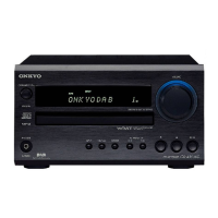
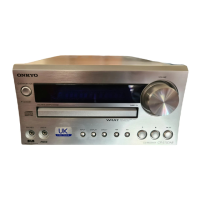
CR-315/315DAB
IC BLOCK DIAGRAMS AND TERMINAL DESCRIPTIONS-6
Q206 : CXD3014R (CD Digital Signal Processor with Built-in RF Amplifier and
Digital Servo + Digital High & Bass Boost + CODEC)-4/4
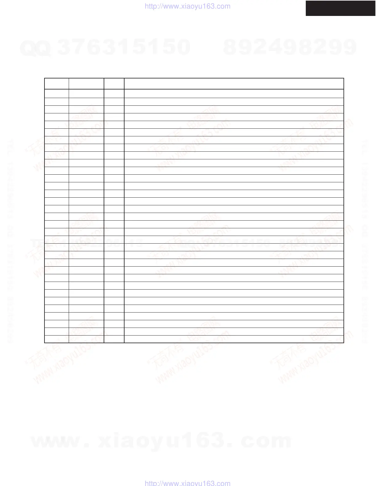
TERMINAL DESCRIPTION (Continued)
Pin No. Pin name I/O Description
88
89
90
91
92
93
94
95
96
97
98
99
100
101
102
103
104
105
106
107
108
109
110
111
112
113
114
115
116
117
118
119
120
TEST1
DATA
CLOK2
DV
SS7
DV
DD7
TEST2
TEST3
TEST4
TEST5
TEST6
DV
SS2
DV
DD2
IOV
DD2
DOUT
TEST
TES1
IOV
SS2
PLLAVD
PLLAVS
XV
SS
XTAO
XTAI
XV
DD
AVD4
AOUT1
VREFL
AVS4
AVS5
VREFR
AOUT2
AVD5
IOV
DD3
IOV
SS3
I
I/O
I
---
---
I
I
O
I
I
---
---
---
O
I
I
---
---
---
---
O
I
---
---
O
O
---
---
O
O
---
---
---
Test mode set.
CPU I/F ARC (DATA).
CPU I/F ARC (CLK).
Internal digital GND.
Internal digital power supply.
Test pin. Normally GND.
Test pin. Normally GND.
Open.
Test pin. Normally GND.
Test pin. Normally GND.
Internal digital GND.
Internal digital power supply.
I/O digital power supply.
Digital Out output.
Test pin. Normally GND.
Test pin. Normally GND.
I/O digital GND.
PLL cell power supply.
PLL cell GND.
Master clock GND.
Crystal oscillation circuit output.
Crystal oscillation circuit input.
Master clock power supply.
Analog power supply.
Lch analog output.
Lch reference voltage.
Analog GND.
Analog GND.
Rch reference voltage.
Rch analog output.
Analog power supply.
I/O digital power supply.
I/O digital GND.
w
w
w
.
x
i
a
o
y
u
1
6
3
.
c
o
m
Q
Q
3
7
6
3
1
5
1
5
0
9
9
2
8
9
4
2
9
8
T
E
L
1
3
9
4
2
2
9
6
5
1
3
9
9
2
8
9
4
2
9
8
0
5
1
5
1
3
6
7
3
Q
Q
TEL 13942296513 QQ 376315150 892498299
TEL 13942296513 QQ 376315150 892498299
http://www.xiaoyu163.com
http://www.xiaoyu163.com
 Loading...