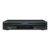
DV-CP702
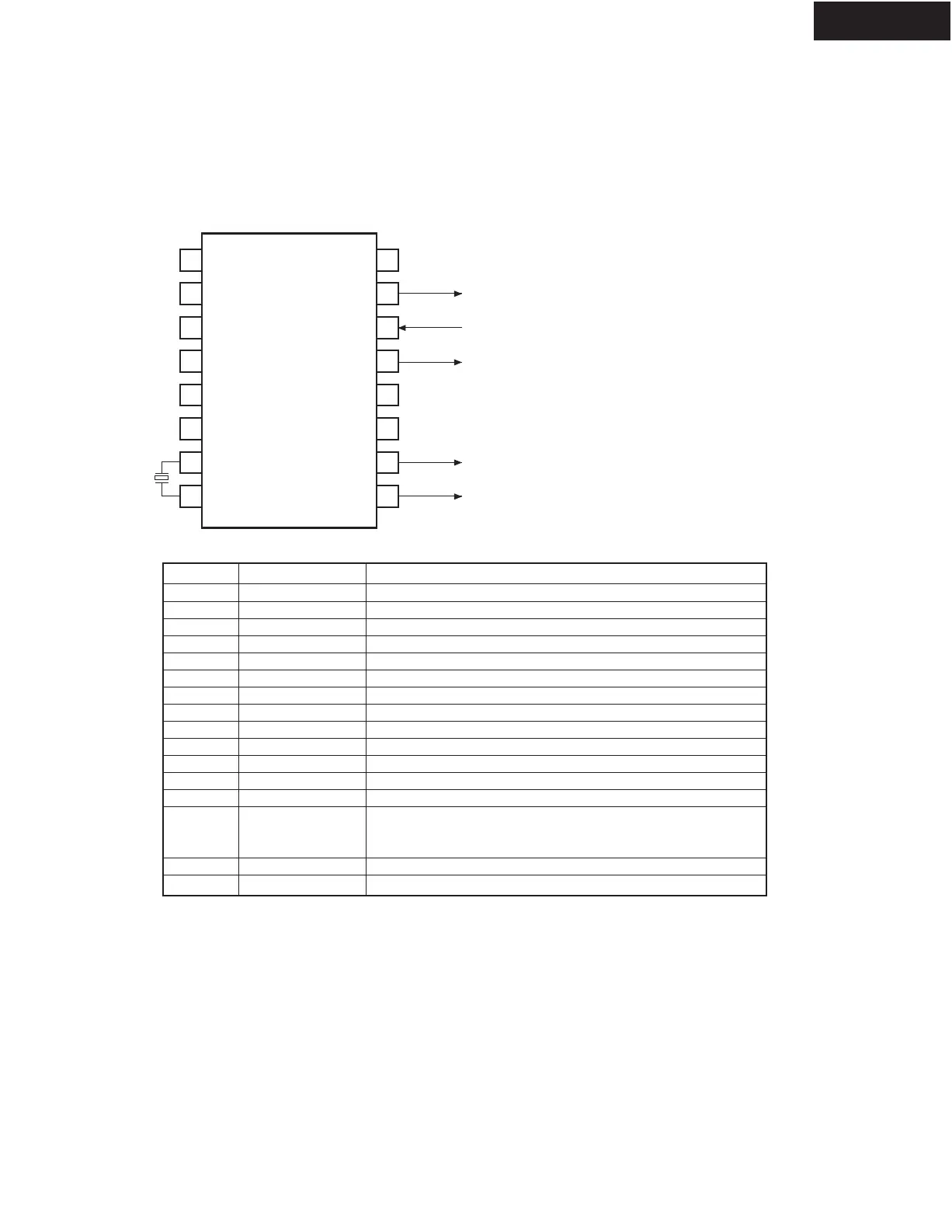
IC BLOCK DIAGRAM/ TERMINAL DESCRIPTION
1
2
3
4
5
6
7
8
VDD2
VSS2
CLK27M
TEST
AVDD
AVSS
XTALOUT
XTALIN
16
15
14
13
12
11
10
9
OE
CLK33M
33.8688MHz
24.576 or 22.5792MHz
16.9344 or 36.864MHz
L or NC (pull up)
16.9344MHz
FSEL1
CLK16M
DVDD
DVSS
CLK512FS
CLKA
Q2601: BU2288FV CLOCK GENERATOR
PIN No.
1
2
3
4
5
6
7
8
9
10
11
12
13
14
15
16
PIN NAME
VDD2
VSS2
CLK27M
TEST
AVDD
AVSS
XTALOUT
XTALIN
CLKA
CLK512FS
DVSS
DVDD
CLK16M
FSEL1
CLK33M
OE
FUNCTION
Digital VDD for 27MHz clock output
Digital GND for 27MHz clock output
27MHz clock output
Output for test
Analog VDD
Analog GND
Standard crystal output
Standard crystal input
Clock output (FSEL1=Open: 16.9344MHz, FEL1=36.864MHz)
Clock output (FSEL1=Open: 22.5792MHz, FEL1=24.576MHz)
Digital GND
Digital VDD
16.9344MHz clock output
Output select: with pull up
Open: 16.9344MHz (9pin), 22.5792MHz (10pin)
L: 36.864MHz (9pin), 24.576Mhz (10pin)
33.8688MHz clock output
Output enable (open: enable, L: disable): with pull up
PIN FUNCTION
PIN CONFIGURATION

 Loading...