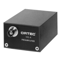
The ORTEC Model 109A Preamplifier is an all-transistor preamplifier designed for nuclear spectroscopy applications. It features pole-zero cancellation and utilizes a field-effect transistor (FET) in its input stage for low-noise performance. The preamplifier is inherently an inverting type, meaning a negative input pulse results in a positive output pulse. It does not perform pulse shaping; instead, it provides a "step" voltage output with an exponential fall time, allowing subsequent main amplifiers to handle system pulse shaping for optimal signal-to-noise ratio.
Function Description:
The 109A's primary function is to convert the charge generated by a detector into a voltage signal suitable for further amplification and processing. It incorporates a charge-sensitive input loop, a voltage amplifier with switch-selectable gain, and a cable driver stage. The charge-sensitive loop, consisting of five transistors (Q1-Q5) acting as an operational amplifier with capacitive feedback, performs the charge-to-voltage conversion. The voltage amplifier (Q6, Q7) then amplifies this signal with a selectable gain of X10 or X1. The cable driver (Q8-Q11) is an impedance converter that ensures the output signal can drive long coaxial cables without significant degradation. A built-in pole-zero cancellation network, determined by C12 and the parallel combination of R17, R18, and R42, sets the output signal's decay time constant to 50 µs, which is crucial for accurate pole-zero cancellation in the subsequent shaping amplifier.
Important Technical Specifications:
- Noise Performance:
- Basis of Warranty: ≤0.025 keV/pF FWHM (Ge) slope, 2.5 keV FWHM (Ge) maximum at 0 pF input capacity.
- Typical Noise (with 2-µs Single RC Main Amplifier):
- 0 pF input capacitance: 2.85 keV FWHM (Si), 2.29 keV FWHM (Ge), 336 rms electrons, 15 ns rise time.
- 50 pF input capacitance: 3.72 keV FWHM (Si), 2.99 keV FWHM (Ge), 440 rms electrons, 25 ns rise time.
- 1000 pF input capacitance: 30.4 keV FWHM (Si), 24.4 keV FWHM (Ge), 3580 rms electrons, 250 ns rise time.
- Slope: 0.0275 keV/pF (Si), 0.022 keV/pF (Ge) for "out" protection; 0.037 keV/pF (Si), 0.0294 keV/pF (Ge) for "in" protection.
- Output Pulse Shape: Exponential fall with 50-µs time constant.
- Integral Nonlinearity: <0.1% for 0-5 V output span with internal series termination.
- Temperature Coefficient: ±0.01%/°C.
- Detector Bias Isolation: 1000 V dc.
- Input Open Loop Gain: >20,000.
- Power Required: +24 V dc at 36 mA, -24 V dc at 36 mA; supplied from ORTEC main amplifier or ORTEC 114/115 Preamplifier Power Supply.
- Power Cable: 10-ft captive power cable.
- Power Connector: Amphenol 17-20090.
- Saturated Output Amplitude: 7 V at end of several hundred feet of unterminated 93Ω cable.
- Output Source Impedance: Adjustable from 50 to 150Ω.
- Charge Sensitivity:
- X10 gain position: 150 mV/MeV (Si), 183 mV/MeV (Ge).
- X1 gain position: 15 mV/MeV (Si), 18.3 mV/MeV (Ge).
- Connectors: DETECTOR, OUTPUT, and TEST Pulse connectors are BNC. DETECTOR BIAS connector is SHV.
- Size: 1.8 x 4 x 6 inches (4.5 x 10.2 x 15.3 cm).
- Weight: Net, 1.5 lb (0.7 kg); gross 2.3 lb (1.1 kg).
- Count Rate with 1% Counting Losses (cts/sec):
- 0.1 MeV (Si Equivalent): 2 x 10^9
- 1 MeV (Si Equivalent): 2 x 10^7
- 10 MeV (Si Equivalent): 2 x 10^5
Usage Features:
- Protection Circuitry: The preamplifier comes with a protection circuit connected "in" by default, making it highly resistant to damage from transients at the Detector Input or Bias Input connectors. This circuit, while causing almost negligible resolution degradation, does not protect the detector itself. The protection circuit can be removed by moving a plug-in jumper from "in" to "out" if the slight degradation is intolerable, but this voids the warranty unless specific precautions are followed.
- Detector Bias: Bias voltage is applied via the SHV connector. A decoupling network (R1, R2, C1) provides approximately 100 MΩ total series resistance. Users must account for voltage drop across this network when biasing leaky detectors. A 10 MΩ parallel bias resistor is provided for very high leakage detectors, reducing the required bias supply voltage but increasing zero pF noise by ~0.5 keV (Si equivalent).
- Input Connection: A direct connection with shielded coaxial cable (preferably 93Ω or 100Ω impedance, such as RG-62/U) should be made between the detector and the front panel DETECTOR BNC connector. Minimizing cable length is crucial for optimal noise performance.
- Output Connection: The preamplifier can drive long 93Ω lines to a shaping main amplifier and is directly compatible with ORTEC transistor main amplifiers.
- Test Pulse Input: A voltage test pulse can be inserted at the rear panel TEST PULSE connector, which has a built-in charge terminator. A 46 mV amplitude at this connector is equivalent to approximately 1 MeV energy loss in a silicon detector. The test pulse can also be inserted into the DET. INPUT connector simultaneously with an operating detector using an external charge terminator, provided it withstands the detector bias voltage.
- Gain Selection: The preamplifier offers two gain positions, X10 and X1. The X10 position typically provides the optimum signal-to-noise ratio.
- Detector Bias Discharge: Before connecting or disconnecting any capacitive device (detector, cable, capacitor, voltmeter probe) to the DET. INPUT connector, the detector bias circuitry must be completely discharged. This involves shorting the DET. BIAS connector on the rear panel for at least 20 seconds. If a variable bias supply is used, turning the voltage control to zero for 20 seconds is sufficient. For battery bias, a short circuit across the DET. BIAS connector is necessary. Crucially, the DET. INPUT on the front panel must NOT be shorted.
Maintenance Features:
- Troubleshooting: If the preamplifier is suspected of malfunctioning, it should be isolated and tested independently. This involves providing a known electrical input signal and observing the output signal with an oscilloscope.
- Performance Testing:
- Input Signal: Use a voltage pulse in the TEST PULSE jack (as described in Section 3.4) or a pulser with a charge terminator at the DET. INPUT jack. The test pulse polarity should match the expected signal input polarity from the detector.
- Output Waveform: Observe the pulse waveform at the OUTPUT jack. For a 460 mV input signal (10 MeV equivalent), expect an output amplitude of ~1.5 V in X10 gain and ~0.15 V in X1 gain.
- Noise Contribution: Verify noise by replacing the detector and associated cables with a capacitor of equal value connected to the DET. INPUT jack. The input jack and capacitors should be electrically shielded (e.g., with aluminum foil for zero capacity testing). Noise performance is measured in conjunction with a main amplifier providing appropriate pulse shaping (typically equal RC differentiation and integration of 2-µs time constants).
- Detector Testing: After verifying preamplifier noise performance, the detector can be tested by duplicating noise tests with the detector connected and normal operating bias applied. The combined noise measurement helps determine the detector's "noise width."
- Circuit Description for Troubleshooting:
- Charge-Sensitive Loop: Provides a fast-rise (~15 ns at 0 pF external capacitance) step voltage with a 400-µs decay. The amplitude at the emitter of Q4 should be ~45 mV per MeV equivalent input signal.
- Voltage Amplifier: Differentiates the Q4 output with a 50-µs time constant (C12). The output at the S1 wiper arm should have a fast rise with a 50-µs decay, with an amplitude 0.34 or 3.4 times greater than at the Q4 emitter, depending on the gain switch.
- Cable Driver: Acts as an impedance converter, providing no gain, and its output signal should mirror the input signal.
- DC Voltages Table: A table of typical DC voltages at various test points (e.g., transistor emitters, bases, collectors, and junction points) is provided to aid in locating defective components. Extreme caution is advised when making these measurements to prevent damage from accidental shorts.
- Replaceable Parts List: A comprehensive list of replaceable parts, including reference designator, part number, description, and manufacturer information, is provided for ordering spare parts. Instructions for ordering unlisted parts are also included.
- Quality Control: Each instrument undergoes stringent quality control tests before shipment, with permanent records maintained for warranty repair and design improvements.
- Repair Service: For repairs, customers must contact ORTEC Customer Services in advance to obtain a Return Authorization Number. Instruments should be packed to withstand normal transit and shipped PREPAID. Damage in transit due to inadequate packing is the sender's responsibility. Out-of-warranty repairs are charged at a standard rate, with notification for gross misuse or mishandling.