2
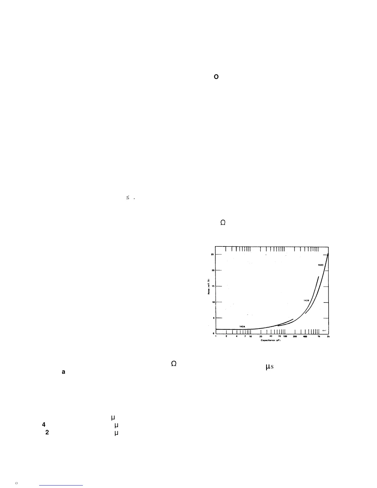
Fig. 2.1. Typical Noise as a Function of
Capacitance Measured with an ORTEC
572 Amplifier and 2-
:
s Time Constant.
2. SPECIFICATIONS
2.1. PERFORMANCE
NOISE (Figs. 2.1 and 2.2)
Detector Maximum
Capacitance Noise
Model (PF) (KeV) (Si)
142A 0 1.60
142A 100 3.40
142B 100 3.20
142B 1000 19.00
142C 400 7.20
142C 1000 14.50
142C 2000 27.00
INTEGRAL NONLINEARITY
#
0.03%
TEMPERATURE INSTABILITY
142A <±50 ppm/°C from 0 to 50°C.
142B <±100 ppm/°C from 0 to 50°C.
142C <±100 ppm/°C from 0 to 50°C.
OPEN LOOP GAIN
142A >40,000
142B >80,000
142C >80,000
CHARGE SENSITIVITY (Si equivalent)
142A Nominally 45 mV/MeV
142B Nominally 20 mV/MeV
142C Nominally 20 mV/MeV
ENERGY RANGE
142A 0 — 200 MeV
142B 0 — 400 MeV
142C 0 — 400 MeV
RISE TIME, 0 to +0.5 V Pulse at E output on 93
S
Load (Fig. 2.3)
142A <5 ns at 0 pF; < 12 ns at 100 pF.
142B <5 ns at 100 pF; < 25 ns at 1000 pF.
142C <11 ns at 400 pF; < 20 ns at 1000 pF.
DECAY TIME
142A Nominally 500
:
s.
142B Nominally 1000
:
s.
142C Nominally 1000
:
s.
RECOMMENDED RANGE OF INPUT
CAPACITANCE
142A 0 to 100 pF.
142B 100 to 400 pF.
142C 400 to 2000 pF.
DETECTOR BIAS VOLTAGE ±1000V maximum.
2.2. INPUTS
INPUT Accepts input signals from semiconductor
charged-particle detector and extends operating
bias to the detector.
BIAS Accepts the detector bias voltage from a
power supply.
TEST Accepts input voltage pulses from a pulse
generator for instrument and system calibration;
R
in
= 93
S
.