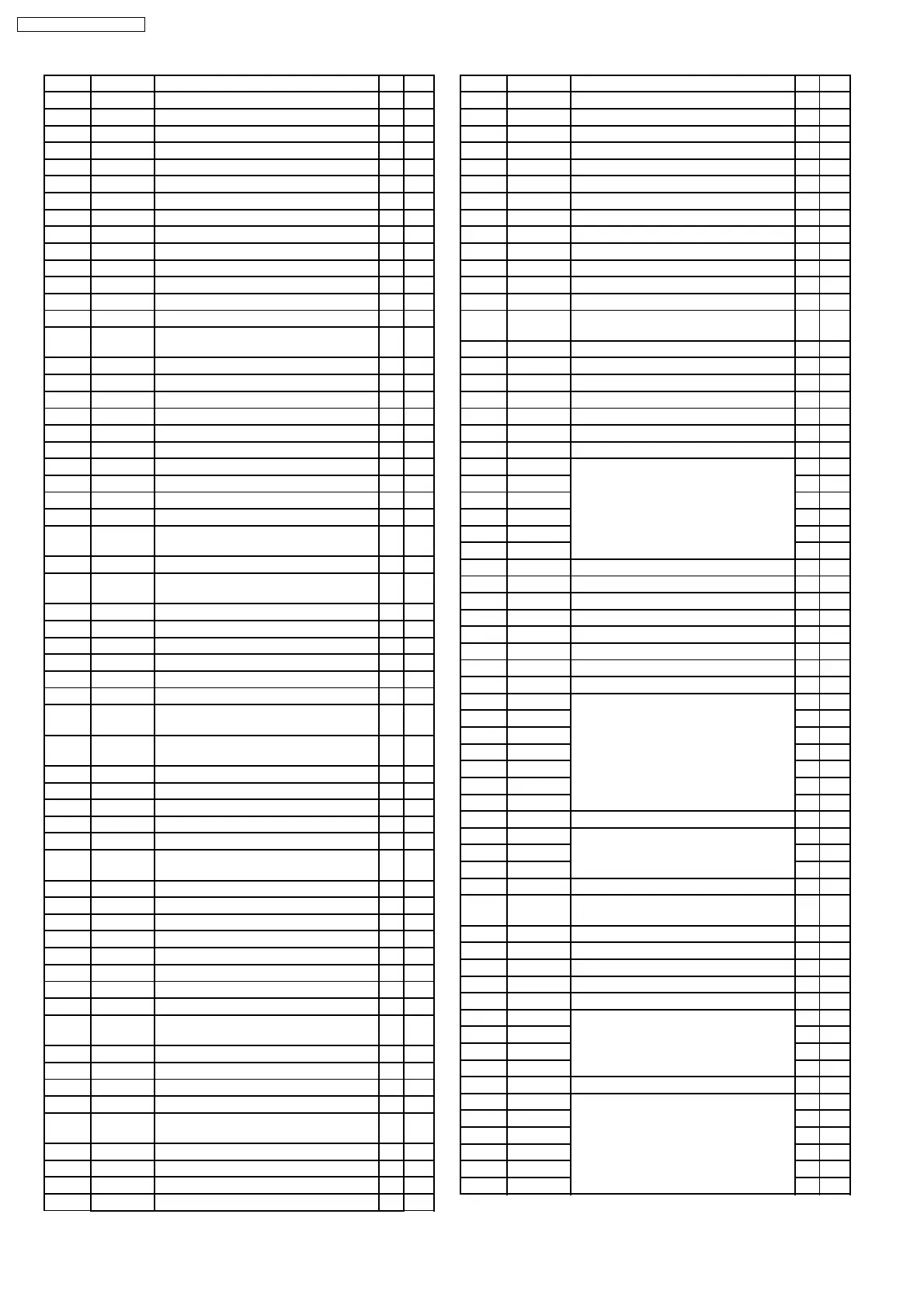
Pin No. Port Descriptions I/O (V)
18 - - - -
19 - - - -
20 nPS FLASH ROM selection signal O 3.3
21 - - - -
22 - - - -
23 R/W Lead/light signal to FLASH ROM O 3.3
24 nMSTRB Memory access signal O 3.3
25 - - - -
26 - - - -
27 MUTE Mute signal output (H:Mute on) O 0
28 - - - -
29 - - - -
30 - - - -
31 SUBO SUBO input I 0
32 - Operation mode setting (external pull-
up)
I 3.3
33 DVDD2 I/O system (3.3V) power supply - 3.3
34 CVSS4 GND - 0
35 (GND) GND I 0
36 - - - -
37 CVSS5 GND - 0
38 - - - -
39 - - - -
40 DVSS2 GND - 0
41 CLK C M AUDIO bit clock input I 1.6
42 SCK Clock input I 3.3
43 LRCK C
M
AUDIO L/R identifying signal input I 1.6
44 CDFS Serial frame sink signal input I 2.6
45 DATA M
C
AUDIO serial data input I 1.6
46 - - - -
47 SI Serial data input I 0
48 CLK M C AUDIO bit clock output O 1.6
49 SCK Clock input I 3.3
50 CVSS6 GND - 0
51 - - - -
52 CVDD3 CORE CPU system (1.6V) power
supply
- 1.6
53 LRCK M
C
AUDIO L/R identifying signal output O 1.6
54 CDFS Serial frame sink signal input I 2.4
55 - - - -
56 DVDD3 I/O system (3.3V) power supply - 3.3
57 DVSS3 GND - 0
58 REST SW Mechanics deck REST SW input I 3.3
59 DATA M
C
AUDIO serial data output O 1.6
60 SO Serial data output O 1.2
61 - - - -
62 - - - -
63 - - - -
64 - - - -
65 - - - -
66 BLKCK Subcode block clock pulse input I 0
67 - - - -
68 DVDD4 CORE CPU system (1.6V) power
supply
- 1.6
69 SW1 Mechanics deck SW1 input I 0
70 CVSS7 GND - 0
71 MCLK Clock output (To Servo DSP) O 3.3
72 DVSS4 GND - 0
73 MLD Command load signal output (To Servo
DSP)
I 3.3
74 MDATA Command data output (To Servo DSP) O 3.3
75 DVDD4 I/O system (3.3V) power supply - 3.3
76 DVSS5 GND - 0
77 - Clock mode setting (L fixation) I 0
Pin No. Port Descriptions I/O (V)
78 - Clock mode setting (H fixation) I 3.3
79 - Clock mode setting (L fixation) I -
80 - - - -
81 SW2 Mechanics deck SW2 input I 0
82 - - - -
83 - - - -
84 - - - -
85 - - - -
86 - - - -
87 - - - -
88 - - - -
89 - - - -
90 CVSS8 GND - 3.3
91 CVDD5 CORE CPU system (1.6V) power
supply
- 0
92 (GND) GND I 1.6
93 DVSS6 GND - 0
94 - - - -
95 CLKENA Oscillation output Cainabl signal O 3.3
96 1 Crystal Connection O 0
97 2 Crystal Connection I 0
98 (VDD) Reset signal input I 1
99 D0 Data base of FLASH ROM I/O 3.4
100 D1 I/O 0
101 D2 I/O 0
102 D3 I/O 0
103 D4 I/O 0
104 D5 I/O 0
105 A16 Address bus of FLASH ROM O 0
106 DVSS7 GND - 0
107 A17 Address bus of FLASH ROM O 3.3
108 A18 O 0
109 A19 Address bus of FLASH ROM O 0
110 A20 O 0
111 CVSS9 GND - 0
112 DVDD5 I/O system (3.3V) power supply - 3.3
113 D6 Data bus of FLASH ROM I/O 0
114 D7 I/O 0
115 D8 I/O 0
116 D9 I/O 0
117 D10 I/O 0
118 D11 I/O 0
119 D12 I/O 0
120 STAT Status signal input I 0.4
121 D13 Data path of FLASH ROM I/O 0
122 D14 I/O 0
123 D15 I/O 0
124 SQCK SOCK clock output(To Servo DPS) O 3.2
125 CVDD6 CORE CPU system (1.6V) power
supply
- 1.6
126 CVSS10 GND - 0
127 - - - -
128 DVSS8 I/O system (3.3V) power supply - 0
129 - - - -
130 DVDD6 I/O system (3.3V) power supply - 3.3
131 A0 Address bus of FLASH ROM O 0
132 A1 O 0
133 A2 O 3.3
134 A3 O 3.3
135 /RST Reset signal output(To Servo DSP) O 3.3
136 A4 Address bus of FLASH ROM O 3.3
137 A5 O 0
138 A6 O 3.3
139 A7 O 3.3
140 A8 O 0
141 A9 O 3.3
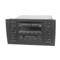
16
CQ-DP383W / CQ-DP383WJ
 Loading...