Do you have a question about the Panasonic KX-TCD410RUM and is the answer not in the manual?
Recommended lead-free solder wire sizes and types for product service.
Identifies the 'PbF' marking on PCBs to indicate lead-free solder.
Shows the 'PbF' mark location on the Base Unit PCB.
Shows the 'PbF' mark location on the Handset PCB.
Shows the 'PbF' mark location on the Charger Unit PCB.
Precautions to prevent recurring malfunctions during repair.
Warning about battery replacement risks and proper disposal.
Instructions for inserting and replacing handset batteries correctly.
Procedure for charging handset batteries before initial use.
Expected talk and standby times for Ni-MH and Ni-Cd batteries.
Steps for replacing handset batteries and selecting battery type.
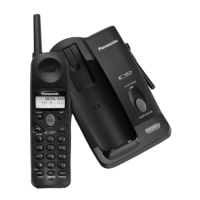
Identifies controls and indicators on the base unit.
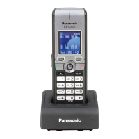
Identifies controls and indicators on the handset.
Steps to connect the base unit and charger unit to power.
Explains symbols used for navigation and display in the service manual.
Procedures for managing Base Unit and Handset PIN codes.
Procedure to reset the base unit PIN to default using a PC.
Resets base unit and handset settings to factory defaults.
How to lock and unlock handset dialling buttons.
Usage of the RECALL button for special telephone services.
How to use the PAUSE function for PBX or long-distance calls.
How to restrict selected phone numbers from being dialled.
Procedure to remove call restriction settings for specific handsets.
How to enable or disable the call barring feature.
Steps to change the language displayed on the handset.
How to select between tone or pulse dialling mode.
How to adjust flash timing based on PBX requirements.
How to store carrier and area codes for automatic route selection.
How to enable or disable the automatic route selection feature.
Overview of direct command functions for programmable settings.
Explains icons and displays shown on the handset screen.
Basic troubleshooting steps before contacting customer support.
Instructions for powering on/off, making/answering calls, and setting clock/date.
Instructions for storing, editing, and dialling using the phonebook.
How to assign phone numbers to hot keys for speed dialling.
Step-by-step guide to disassemble the base unit.
Step-by-step guide to disassemble the handset.
Step-by-step guide to disassemble the charger unit.
Cautionary note regarding proper assembly of the base unit's CHG terminal.
Flowchart for diagnosing and resolving common issues.
Steps to check power supply and voltage levels on base unit and handset.
Procedure to check battery charging status on base unit, handset, and charger.
Steps to verify the base unit's and handset's link capability.
How to check the microphone and transmission signal route.
How to check the speaker and reception signal route.
How to check the Caller ID function via the signal route.
Steps to check bell signal reception at the base unit and handset.
List of equipment, JIGs, and PC setup for base unit checks.
List of equipment, JIGs, and PC setup for handset checks.
Detailed adjustment procedures for base unit components (A-N).
Procedure to check charging voltage on the charger unit.
Shows component layout for base unit adjustment procedures.
Shows flow solder side view for charger unit adjustment procedures.
Detailed adjustment procedures for handset components (A-P).
Shows the layout for handset adjustment procedures.
RF specifications for the base unit.
RF specifications for the handset.
Procedure for checking the handset speaker using a voltmeter.
Table of transmit and receive frequencies for base unit and handset.
Schematic block diagram of the base unit's functional modules.
Schematic block diagram of the handset's functional modules.
Overview of the base unit's circuit components and functions.
Explanation of the power supply circuit for the base unit.
Description of the telephone line interface circuit.
Explanation of the transmitter and receiver blocks in the base unit.
How the pulse dialing function operates.
Description of the FLASH PROM's function and interface.
Overview of the handset's circuit components and functions.
Explanation of the handset's power supply and reset circuit.
Explanation of the handset's battery charging circuit.
How the handset detects low battery or power down conditions.
Power supply circuit diagram for the charger unit.
Table showing signal paths for various functions.
Pinout and description for the Base Unit BBIC (IC2).
Pinout and description for the Handset BBIC (IC1).
Purpose and introduction to the base unit's serial EEPROM parameters.
EEPROM addresses for general setup parameters on the base unit.
EEPROM addresses for switch control settings on the base unit.
EEPROM settings for flash time configuration.
EEPROM addresses for Caller ID configuration settings.
EEPROM addresses for Base Unit UI task configurations.
Purpose and introduction to the handset's serial EEPROM parameters.
EEPROM addresses for general setup parameters on the handset.
EEPROM addresses for signal detection settings (factory use).
EEPROM addresses for battery-related parameters.
EEPROM addresses for default audio parameter settings.
EEPROM addresses for volume setting configurations.
Preparation steps for replacing flat package ICs, including solder.
Step-by-step procedure for soldering flat package ICs.
Procedure to modify bridged pins during IC replacement.
Diagram showing parts location for the base unit cabinet.
Diagram showing parts location for the handset cabinet.
Diagram showing parts location for the charger unit cabinet.
List of accessories and packing materials for the KX-TCD410 model.
List of accessories and packing materials for the KX-TCD412 model.
List of accessories and packing materials for the KX-A142 model.
List of fixtures and tools required for service procedures.
Terminal guide for ICs, transistors, and diodes on the base unit.
Terminal guide for ICs, transistors, and diodes on the handset.
Terminal guide for ICs, transistors, and diodes on the charger unit.
List of replacement cabinet, electrical, and PCB parts for the base unit.
List of replacement cabinet, electrical, and PCB parts for the handset.
List of replacement parts for the charger unit cabinet and PCB.
Detailed schematic diagram of the base unit's circuitry.
Detailed schematic diagram of the handset's circuitry.
Detailed schematic diagram of the charger unit's circuitry.
Shows the component layout on the base unit's circuit board.
Shows the flow solder side view of the base unit's circuit board.
Shows the component layout on the handset's circuit board.
Shows the flow solder side view of the handset's circuit board.
Shows the component layout on the charger unit's circuit board.
Shows the flow solder side view of the charger unit's circuit board.