EasyManua.ls Logo

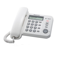
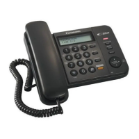
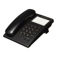
Panasonic KX-TS550LXB User Manual

Panasonic KX-TS550LXB
11 pages
To Next Page IconTo Next Page
Page #1 background imageLoading...
Page #1 background image
1 CHANGES (for RoHS) 2
1.1. SUBJECT
2
2 REPLACEMENT PARTS LIST
3
2.1. REFERENCE CHART
3
2.2. ORIGINAL AND NEW PARTS COMPARISON LISTS
4
3 CORRECTION
6
3.1. CABINET AND ELECTRICAL PARTS LOCATION
(Changed from original section 14 CABINET AND
ELECTRICAL PARTS LOCATION)
6
© 2006 Panasonic Communications Co., Ltd. All
rights reserved. Unauthorized copying and
distribution is a violation of law.
KX-TS550LXB
KX-TS550LXW
Integrated Telephone System
Black Version
White Version
(for Latin America)
3.2. SCHEMATIC DIAGRAM (Changed from original section
19 SCHEMATIC DIAGRAM)
7
3.3. Main (Component View) (Changed from original section
20.1. Main (Component View))
9
3.4. Main (Flow Solder Side View) (Changed from original
section 20.2. Main (Flow Solder Side View))
10
Telephone Equipment
Please file and use this supplement manual together with the service manual mentioned below.
CONTENTS
Page Page
ORDER NO. KM40607177SE
Question and Answer IconNeed help?

Do you have a question about the Panasonic KX-TS550LXB and is the answer not in the manual?

Panasonic KX-TS550LXB Specifications

General IconGeneral
BrandPanasonic
ModelKX-TS550LXB
CategoryTelephone
LanguageEnglish

Summary

RoHS Compliance Changes

Subject of RoHS Changes

Details the introduction of RoHS-compliant parts and their implications for product servicing.

Replacement Parts Information

Parts Reference Chart

Defines reasons for part changes and interchangeability codes for original and new parts.

Original and New Parts Comparison

Lists changes in part suffixes for the base unit, including reasons for modification.

Technical Corrections and Updates

Cabinet and Parts Location Update

Updates cabinet and electrical parts location, specifying screw types and dimensions.

Updated Schematic Diagram

Presents the revised circuit schematic diagram with component labels and connections.

Main PCB Component Layout

Illustrates the component placement and identification on the main printed circuit board.

Main PCB Solder Side View

Shows the flow solder side of the main PCB, detailing component placement and routing.
Related product manuals