Pin No. Mark I/O Function
96 MONI5 I/O Inside/ Internal Monitor 1
Exterior/ Outside Memory Data 1
General Use Port 32
Digital Video Output 1
Stream Error Flag Output
97 MONI4 I/O Inside/ Internal Monitor 0
Exterior/ Outside Memory Data 0
General Use Port 31
Digital Video Output 0
Stream Sector Head Output
98 MONI3 - Analog power Supply
99 MONI2 O DRCVCO Use Capacity
Connection 1
100 MONI1 - Analog GND
101 MONI0 O DRC Use ADC Voltage (Top)
102 AVDDD O DRC Use ADC Voltage (MDL)
103 PLFIL1 O DRC Use ADC Voltage (BTM)
104 AVSSD O INLINE CAPA Use Capacity
Connection
105 VREFH7 - Analog Ground
106 VREFL7 O INLINE DATA Use Capacity
Connection
107 CCAPA - Analog Power Supply
108 AVSSC O Inside Analog Monitor 1
109 CDATA O Inside Analog Monitor 2
110 AVDDC I Exterior/ Outside RF Input (-)
111 ANAMONI1 I Exterior/ Outside RF Input (+)
112 ANAMONI2 I RF Input 6
113 RFINN I RF Input 5
114 RFINP I RF Input 4
115 VIN1RF I RF Input 3
116 VIN2RF I RF Input 2
117 VIN4RF I RF Input 1
118 VIN3RF - Analog Power Supply
119 AVDDB I 5 Bits Standard Voltage (H)
120 VREFH5 I 5 Bits Standard Voltage (M)
121 VREFL5 I 5 Bits Standard Voltage (L)
122 AVSSB - Analog GND
123 LPC1 I DVD LPC Input
124 LPC01 O DVD LPC Output
125 LPC2 I CD LPC Input
126 LPC02 O CD LPC Output
127 VREFH O Standard Voltage 2.20 V Output
128 VHALF O Standard Voltage 1.65 V Output
129 VIN10 I CD Head Input
130 VIN9 I CD Head Input
131 VIN5 I DVD Head Input
132 VIN6 I DVD Head Input
133 VIN7 I CD Head Input
134 VIN8 I CD Head Input
135 VIN3 I DVD Head Input
136 VIN4 I DVD Head Input
137 VIN2 I DVD Head Input
138 VIN1 I DVD Head Input
139 AD0 I General Use AD Input (BSDA
Offset Revision TK Use)
140 AD1 I General Use AD Input
141 AD2 - Analog power Supply
142 AD4 O AD Self Bias Reference Low-side
143 ADSSH I General Use AD Input
144 PWM1 O AD Self Bias Reference Hi-side
145 PWM0 - Analog GND
146 AVDDH I JFVCO Control Voltage (include
iRAM Edition)/
General Use AD Input (BSDA
Offset Revision FC Use)
147 DAC3OUT O Tracking Drive Output
148 DAC2OUT O Focus Drive Output
149 DAC1OUT O Y (Brightness)/ G (Green) Analog
Signal
Pin No. Mark I/O Function
150 AVDDF - DAC Use Power Supply
151 COMP1 O Cb (Colour Difference)/ B (Blue)
Analog Signal
152 VREF O Cr (Colour Difference)/ R (Red)
Analog Signal
153 IREF1 I Inside/ Internal DAC Reference
Voltage
154 COMP2 I Inside/ Internal DAC Bias Current
Setting Use Resistance Terminal
155 AVSSF I Inside/ Internal DAC Stabilizer
Capacity Connection Terminal
156 DAC4OUT O Y (Brightness)/ Comp (Composite)
Analog Terminal
157 DAC5OUT - DAC Use GND
158 AVDDE O C (Colour) Analog Signal
159 AVSSE - PLL Use Power Supply
160 AVDDG - PLL Use GND
161 AVSSG PLL Use Power Supply
162 OSCI - PLL Use GND
163 OSCO O Audio Clock Phase Difference/
Stream Data Output 7
164 VSS - GND
165 VDD12 I Oscillation Input (27 MHz/54 MHz)
166 DACCK O Oscillation Output (27 MHz/54
MHz)
167 LRCK - I/O Power Supply
168 SRCK I/O Exterior Audio Clock
Stream Clock Output
169 ADOUT3 O LR Channel Clock
Stream Data Output 6
170 ADOUT2 O Bits Clock/ Stream Data Output 5
171 ADOUT1 O Audio Down Mix
Stream Data Output 4
172 ADOUT0 - Logic Power Supply
173 IECOUT - GND
174 VSS O Audio Data
Inside/ Internal Monitor 11
Stream Data Output 3
175 VDD33 O Audio Data
Inside/ Internal Monitor 10
Stream Data Output 2
176 VDIO7 O Audio Data
Inside/ Internal Monitor 9
Stream Data Output 1
177 VDIO6 O IEC958 Digital Audio Data
Inside/ Internal Monitor 8
Stream Data Output 0
178 VDIO5 - I/O Power Supply
179 VDIO4 - GND
180 VDIO3 I/O Debug Use Input Clock
Stream Sector Head Output
181 VDIO2 I/O Debug Use Input Output Trigger
Exterior Memory Data 15
General Port/ Mode Setup Data
182 VDIO1 I/O Debug Use Input Output Data
Stream Error Flag Output
183 VDIO0 I/O Debug Use Input Output Trigger 1
Exterior Memory Data 14
General Port 28
Mode Setup Clock
184 VDD33 I/O Debug Use Output Trace Clock
Exterior Memory Data 13
General Port 29
185 VSS I/O Debug Use Input Output Trace
Data 0
Exterior Memory Data 12
General Port 23
186 EXTRG1 I/O Debug Use Input Output Trace
Data 1
Exterior Memory Data 11
General Port 24
87
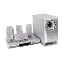
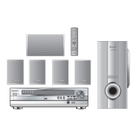
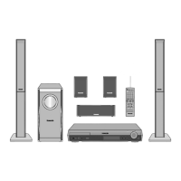
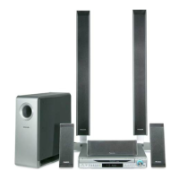
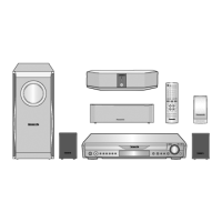
SA-HT535E / SA-HT535EG
 Loading...