Do you have a question about the Philips 32PFL4007D/78 and is the answer not in the manual?
Outlines the technical parameters and specifications of the television set.
Provides guidance on how to use the television set, including download links.
Details all available input and output connectors on the TV.
Provides an overview of the chassis, referring to block diagrams for PWB locations.
Describes the connectors located on the side panel of the television.
Describes the connectors located on the rear panel of the television.
Details critical safety regulations and precautions for repair.
Highlights important warnings regarding ESD, high voltage, and component replacement.
Provides general notes on measurements, waveforms, and specific conditions.
Lists and defines technical abbreviations used throughout the manual.
Illustrates the correct routing and dressing of internal cables.
Specifies the recommended positions for servicing the TV set.
Details the process for removing and assembling internal components and the panel.
Outlines the steps for re-assembling the television set after repair.
Identifies key test points and conditions for diagnosing the set.
Explains various service modes (SDM, SAM, Factory, CSM, ComPair) for diagnostics and alignment.
Illustrates the power-on sequence and state transitions of the TV.
Introduces ComPair, a diagnostic and repair tool for Philips products.
Details the procedure for upgrading the TV's main software via USB.
Explains error codes and how to read the error buffer for fault diagnosis.
Describes how to interpret LED blinking patterns for error indication.
Provides practical advice and tips for fault finding and repair actions.
Introduces the TPM9.2L LA platform and its key components.
Describes the power supply architecture and units used in the chassis.
Explains the function and voltages provided by the DC/DC converters.
Details the tuner and demodulator circuitry for analogue and digital TV reception.
Describes the implementation of the HDMI multiplexer and its configuration.
Explains the main video and audio processor and its features.
Covers the back-end processing integrated into the main processor.
Provides data sheet details for the TPS54319 power management IC.
Provides data sheet details for the STA381BW audio amplifier IC.
Provides data sheet details for the MT5366SVOG/B GPIO interface IC.
Provides data sheet details for the CXD2828ER ISDB-T demodulator IC.
Provides data sheet details for the RTL8201EL Ethernet controller IC.
Shows the wiring layout for the 32-inch 4000 series model.
Shows the wiring layout for the 42-inch 4000 series model.
Provides a functional block diagram of the 4000 series system.
Circuit diagram and PWB layout for the PSU board (32"/37" models).
Circuit diagram and PWB layout for the PSU board (42" models).
Circuit diagram for the SSB board used in 3000/3500/4000 series.
Circuit diagram for side AV, USB, and PC audio input connections.
Circuit diagram detailing the HDMI connector pinouts and configurations.
Circuit diagram for the HDMI switch IC and its connections.
Circuit diagram for the DDR3 DRAM modules.
Circuit diagram for flash memory, crystal, JTAG, and UART components.
Circuit diagram for the audio amplifier, headphone, and subwoofer circuitry.
Circuit diagram for the A/V interface and analog signal processing.
Circuit diagram for GPIO interface, IR, and keyboard control signals.
Circuit diagram for the LVDS output to the display panel.
Circuit diagram for the RS-232 communication interface.
Circuit diagram for the tuner module and its power supply.
Circuit diagram for the ISDB-T demodulator IC.
Circuit diagram for the Ethernet controller and RJ45 connector.
Top side physical layout of the SSB board.
Bottom side physical layout of the SSB board.
Circuit diagram for the IR/LED board.
Circuit diagram for the keyboard control panel.
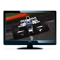
Styling and part identification for the 32PFL4017G model.
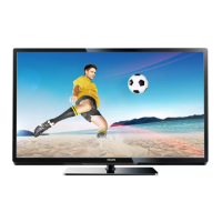
Styling and part identification for the 42PFL4007G model.