Published by LX-KM 1036 AVM Printed in the Netherlands
DCD322/12
Subject to modi cation EN
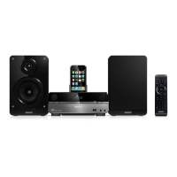
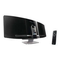
DVD Micro System
Contents
Page
Contents
Page
©
Copyright 2010 Philips Consumer Electronics B.V. Eindhoven, The Netherlands.
All rights reserved. No part of this publication may be reproduced, stored in a
retrieval system or transmitted, in any form or by any means, electronic,
mechanical, photocopying, or otherwise without the prior permission of Philips.
Version 1.1
1 Technical Specification and Connection Facilities and
Version Variation
2 Laser Beam Safety Precautions.................................2-1
3 Important Safety Precautions ..........................3-1 to 3-2
4 Safety Check After Servicing .................................... 4-1
6 Standard Notes For Servicing,Lead Free Requirements
& Handling Flat Pack IC ..................................6-1 to 6-4
5 Safety Information General Notes & Lead Free
7 Direction of Use ...............................................7-1 to 7-5
8 Cabinet Disassembly Instructions ................... 8-1 to 8-2
12 AMP Board
9 Troubleshooting .............................................. 9-1 to 9-2
10 Block Diagram ........................................................10-1
11 Wiring Diagram ...................................................... 11-1
13 Display Board
14 Headphone and USB Board
Layout Diagram ................................12-5
15 Power Board
16 IPOD Board
18 Exploded View......................................................13-1
19 Revision List .........................................................14-1
17 Decoder Board
Circuit Diagram ...............................12-6 to 12-7
Circuit Diagram ..............................12-9
Circuit Diagram ..............................12-10 to 12-13
Layout Diagram ...............................12-8
Layout Diagram .............................12-9
Layout Diagram .............................12-14
...................................................1-1 to 1-2
Circuit Diagram .................................12-1
Layout Diagram ................................12-2
Circuit Diagram .................................12-3
Circuit Diagram .................................12-5
Layout Diagram ................................12-4
Requirements ............................................................5-1
3141 785 35501
Recor dable
ReW ritable