EasyManua.ls Logo

Philips HTS3100/98 - User Manual

Philips HTS3100/98
49 pages
Print Icon
To Next Page IconTo Next Page
Loading...
Published by KC-TE 0635 AV Systems Printed in the Netherlands Subject to modification EN 3139 785 31871
HTS3100/05/12/51/75/93/98
DVD Receiver
CLASS 1
LASER PRODUCT
1 Technical Specifications and Connection
Facilities 2
2 Measurements Setup, Service Aid &
Lead Free Requirements 4
3 Service Hints 8
4 Directions For Use 9
5 Dismantling Instructions & Service Positions 11
6 Service Test Program 14
7 Block Diagram and Wiring Diagram 17
Block Diagram 17
Wiring Diagram 18
8 Circuit Diagram and PWB Layout 19
Front: Display 19
Front: Display (Top view) 20
Front: Display (Bottom view) 21
Front: Standby 22
Front: Standby (Top View) 22
Front: Standby (Bottom View) 22
MKI
Mono Board: Circuit Diagram (Part 1) 23
MKI
Mono Board: Circuit Diagram (Part 2) 24
©
Copyright 2006 Philips Consumer Electronics B.V. Eindhoven, The Netherlands.
All rights reserved. No part of this publication may be reproduced, stored in
a retrieval system or transmitted, in any form or by any means, electronic,
mechanical, photocopying, or otherwise without the prior permission of Philips.
Version 1.1
Contents PageContents Page
MKI
Mono Board: Circuit Diagram (Part 3) 25
MKI
Mono Board: Circuit Diagram (Part 4) 26
MKI
Mono Board: Circuit Diagram (Part 5) 27
MKI
Layout: Mono Board (Top View) 28
MKI
Layout: Mono Board (Bottom View) 29
MKII
Mono Board: Circuit Diagram (Part 1) 30
MKII
Mono Board: Circuit Diagram (Part 2) 31
MKII
Mono Board: Circuit Diagram (Part 3) 32
MKII
Mono Board: Circuit Diagram (Part 4) 33
MKII
Mono Board: Circuit Diagram (Part 5) 34
MKII
Layout: Mono Board (Top View) 35
MKII
Layout: Mono Board (Bottom View) 36
PSU Circuit Diagram 37
8 Overview - Modulator, Input/Output and
Headphone/Line Output Connectors 41
TAS5086-5142V6REF 41
Power Output Stage (SE) 42
Power Output Stage (BTL) 43
Power Supplies 44
Amp Board Layout : Topview 45
Amp Board Layout : Bottomview 46
9 Exploded View & Spare Parts List 47
Exploded View of the set 47
Spare Part List 48
10 Revision List 49
This Service manual is for HTS3100/05/12/51/75/93/98 First and Second
Generation models.
For First Generation model (HTS3100/05/12/51/93/98), the serial number
begins with NW1A xxxx xxxx (PSCI) and VN1A xxxx xxxx (PACH).
For Second Generation model (HTS3100/05/12/51/75/93/98), the serial number
begins with NW2A xxxx xxxx (PSCI) and VN2A xxxx xxxx (PACH).
Question and Answer IconNeed help?

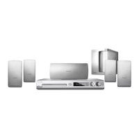
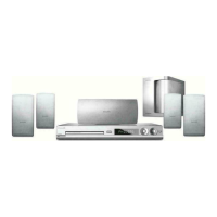
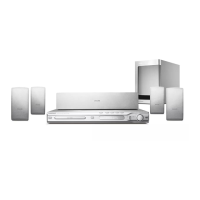
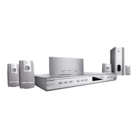
Do you have a question about the Philips HTS3100/98 and is the answer not in the manual?

Summary

Specifications

General Specifications

Covers general electrical and physical specifications of the DVD receiver.

Measurements Setup, Service Aid & Lead Free Requirements

Measurement Setup Procedures

Outlines the equipment and procedures for testing various components.

Handling Chip Components

Provides guidelines for safely dismounting, mounting, and soldering chip components.

ESD Protection Measures

Explains electrostatic discharge risks and protection measures for sensitive components.

Lead Free Solder Requirements

Details the specifications and procedures for working with lead-free solder.

Dismantling Instructions

Service Test Program

Display Test Procedures

Details patterns and procedures for testing the display functionality.

Block Diagram

Wiring Diagram

Circuit Diagram and PWB Layout

MKI Mono Board: Circuit Diagram Part 1

Part 1 of the circuit diagram for the MKI Mono Board.

MKI Mono Board: Circuit Diagram Part 2

Part 2 of the circuit diagram for the MKI Mono Board.

MKI Mono Board: Circuit Diagram Part 3

Part 3 of the circuit diagram for the MKI Mono Board.

MKI Mono Board: Circuit Diagram Part 4

Part 4 of the circuit diagram for the MKI Mono Board.

MKI Mono Board: Circuit Diagram Part 5

Part 5 of the circuit diagram for the MKI Mono Board.

MKII Mono Board: Circuit Diagram Part 1

Part 1 of the circuit diagram for the MKII Mono Board.

MKII Mono Board: Circuit Diagram Part 2

Part 2 of the circuit diagram for the MKII Mono Board.

MKII Mono Board: Circuit Diagram Part 3

Part 3 of the circuit diagram for the MKII Mono Board.

MKII Mono Board: Circuit Diagram Part 4

Part 4 of the circuit diagram for the MKII Mono Board.

MKII Mono Board: Circuit Diagram Part 5

Part 5 of the circuit diagram for the MKII Mono Board.

PSU Circuit Diagram (Europe)

Circuit diagram for the European Power Supply Unit.

PSU Circuit Diagram (AP)

Circuit diagram for the AP (American/Asian) Power Supply Unit.

Exploded View & Spare Parts List

Philips HTS3100/98 Specifications

General IconGeneral
BrandPhilips
ModelHTS3100/98
CategoryReceiver
LanguageEnglish

Related product manuals