LTE Standard Module Series
EC200T Series Hardware Design
EC200T_Series_Hardware_Design 48 / 90
Table 16: Pin Definition of PCM and I2C Interfaces
Pin Name Pin No. I/O Description Comment
PCM_DIN 24 DI PCM data input
1.8 V power domain.
If unused, keep it open.
PCM_DOUT 25 DO PCM data output
1.8 V power domain.
If unused, keep it open.
PCM_SYNC 26 IO
PCM data frame
sync
1.8 V power domain.
In master mode, it serves as an output signal.
In slave mode, it is used as an input signal.
If unused, keep it open.
PCM_CLK 27 IO PCM clock
1.8 V power domain.
In master mode, it serves as an output signal.
In slave mode, it is used as an input signal.
If unused, keep it open.
I2C_SCL 41 OD I2C serial clock
Used for external codec.
An external 1.8 V pull-up resistor is required.
If unused, keep it open.
I2C_SDA 42 OD I2C serial data
Used for external codec.
An external 1.8 V pull-up resistor is required.
If unused, keep it open.
Clock and mode can be configured by AT command, and the default configuration is short frame
synchronization format with 2048 kHz PCM_CLK and 8 kHz PCM_SYNC.
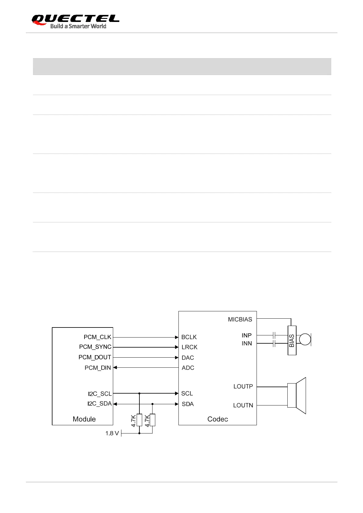
The following figure shows a reference design of PCM interface with external codec IC.
Figure 22: Reference Circuit of PCM Application with Audio Codec
 Loading...


